What is high-tech PCB manufacturing? Let’s discover its manufacturing products types, production process and technology, design specification, difference between traditional PCB.
Are you troubled with these problems?
- Is your PCB suffering from signal attenuation due to uncontrolled impedance in high-frequency, high-speed scenarios?
- Are long lead times and high costs disrupting your rhythm when dealing with multi-variety, small-batch orders?
- Is thermal management failing due to material mismatch in complex multilayer stack-up designs?
As a high-tech PCB manufacturer, Best Technology can provide you service and solution:
- Smart Impedance Control System – Dynamic calibration from design to mass production ensures ±3% impedance accuracy for lossless high-frequency signal transmission.
- Agile Manufacturing Line – Modular production units enable flexible combination, delivering small-batch orders within 72 hours while cutting costs by 20%.
- Thermal Management Expertise – Optimized material stack-up via thermal simulation, paired with thermal interface materials, resolves heat dissipation challenges in high-power PCBs.
Welcome to contact us if you have any inquiry for high-tech PCB manufacturing: sales@bestpcbs.com.
What Is High-Tech PCB Manufacturing?
High-tech PCB manufacturing uses high-frequency materials (such as PTFE substrates with a dielectric loss of ≤0.004), micromachining technology (laser drilling aperture <75μm / mSAP line width <30μm) and arbitrary layer interconnection processes.
Through full process automation control (AOI accuracy ±12μm / layer deviation ≤25μm), we produce high-density (line width/spacing ≤40μm), high reliability (compliant with IPC-6012 Level 3 standards), and high signal integrity (insertion loss <0.3dB/inch@28GHz) printed circuit boards that meet the core requirements of high-end electronic devices such as 5G/6G communications, AI computing chips, and autonomous driving systems.
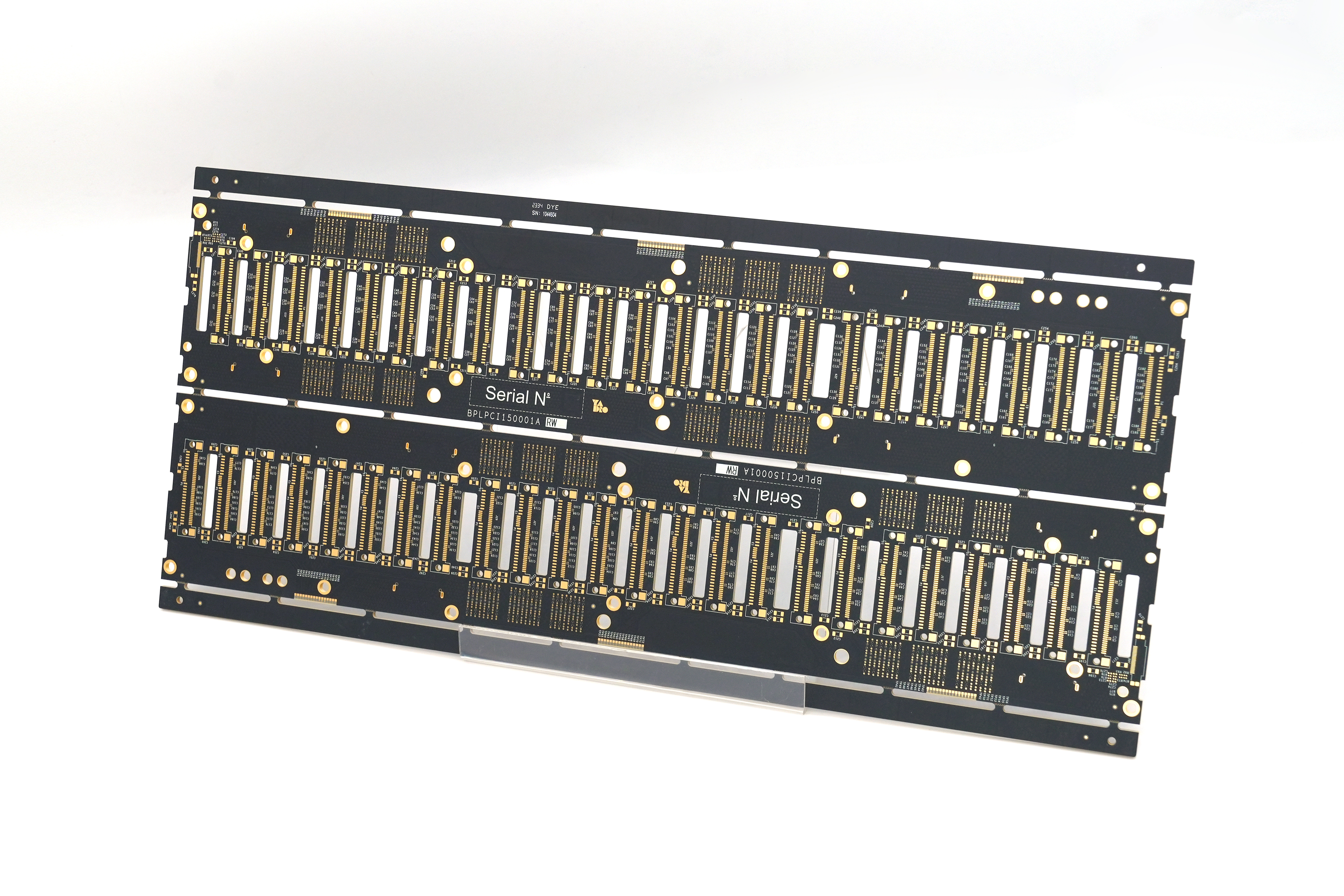
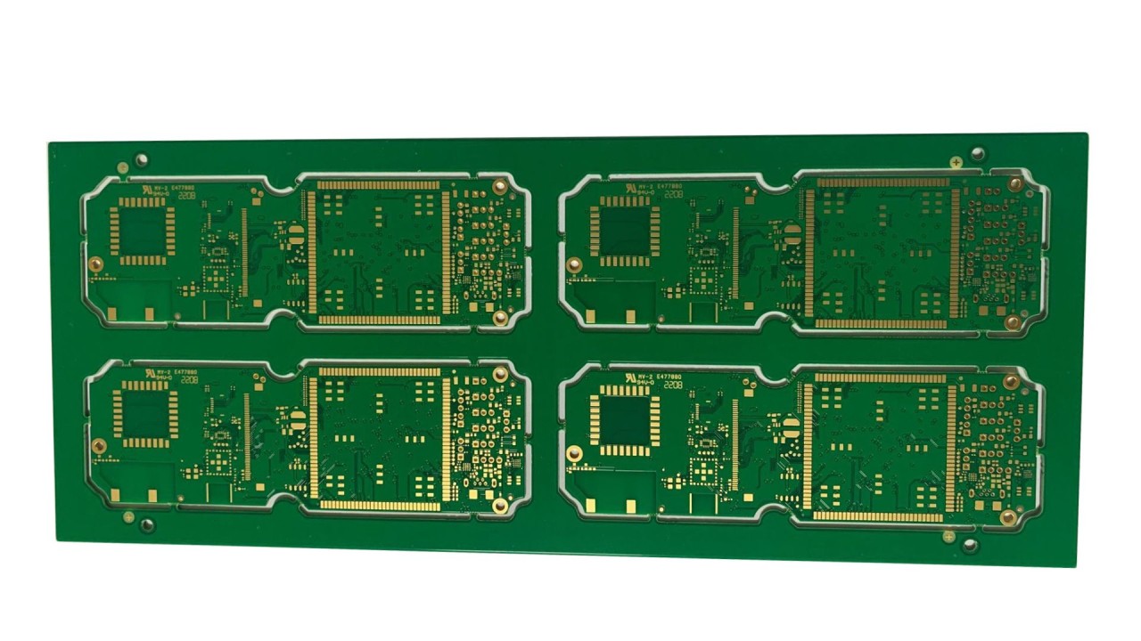
Types of High-Tech PCB Manufacturing Products
Rigid PCB
- Characteristics: Non-flexible substrates (fiberglass cloth/epoxy resin/ceramic), high mechanical strength and support.
- Classifications: Single/Double-Sided Boards; Multilayer Boards (4-30+ layers); High-Layer Multilayer Boards (18+ layers)
- Applications: Consumer electronics, computers, industrial control.
Flexible PCB (FPC)
- Characteristics: Polyimide flexible substrate, bendable and foldable, adaptable to 3D spatial layouts.
- Advantages: Lightweight, strong dynamic application adaptability (TWS earphones, smartwatches).
- Applications: Wearable devices, automotive displays, medical endoscopes.
Rigid-Flex PCB
- Characteristics: Combines rigid support and flexible bendability, reduces connector failure risks.
- Applications: AR glasses, industrial robot joints, humanoid robot modules.
High-Frequency PCB
- High-Frequency Boards: Low dielectric loss materials (Rogers 4350B), used in 5G base stations, satellite communications.
- Characteristics: Precise impedance control, adaptable to GHz-level signal transmission.
High-Density Interconnect (HDI) Boards
- Technologies: Laser microvias (diameter ≤ 100μm), blind/buried vias, any-layer interconnection (Anylayer).
- Advantages: Line width/spacing ≤ 40μm, adaptable to smartphones, wearables, Mini LED backlight modules.
Metal Core PCB (MCPCB)
- Aluminum Substrate: Excellent heat dissipation, used in LED lighting, photovoltaic inverters.
- Copper Substrate: Thermal conductivity 380W/mK, applied in high-power LEDs, high-speed rail traction converters.
- Stainless Steel Substrate: Corrosion-resistant, used in marine monitoring equipment.
- Characteristics: Strong thermal management capability, suitable for high-power scenarios.
Ceramic Substrate
- Alumina: Thermal conductivity 24-28W/mK, used in laser packaging, spacecraft power modules.
- Aluminum Nitride: Thermal conductivity 170-230W/mK, applied in IGBT modules, 5G RF devices.
- Advantages: High thermal stability, low expansion coefficient, suitable for high-temperature extreme environments.
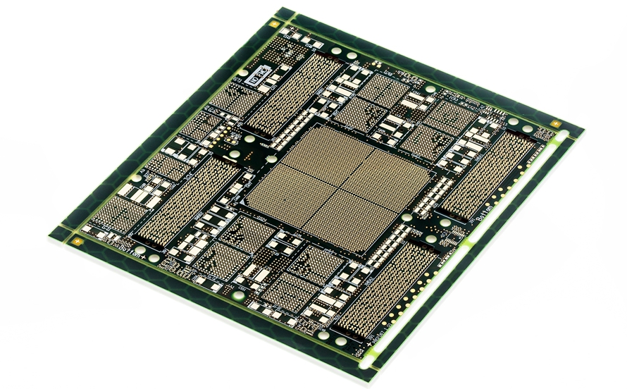
Specialty PCB
- IC Substrate: Line width/spacing ≤ 2μm, supports chip-level packaging (e.g., TSMC CoWoS, Samsung HBM3).
- Thick Copper Boards: Copper thickness ≥ 3oz, carries high current (50A+), used in industrial power supplies, EV charging piles.
- Halogen-Free PCB: Environmental standards (halogen ≤ 900ppm), suitable for EU export electronics.
Package Substrate
- Functions: Directly mounts chips, provides electrical connections, heat dissipation, and protection.
- Technologies: Micro blind vias (diameter ≤ 30μm), BT/ABF materials, supports AI chips, memory chip packaging.
High-Tech PCB Manufacturing Processes
1. Cutting and Substrate Preparation
- Substrate Selection: High-precision FR-4 epoxy glass cloth substrate with copper foil thickness 12-35μm, subjected to constant temperature and humidity treatment (23℃±2℃, humidity 50%±5%) to eliminate internal stress. Cutting size deviation controlled within ±0.1mm, diagonal error ≤0.2mm, edge chamfer radius 0.5-1mm to prevent scratches.
- Surface Treatment: Cleanliness tested via water film method (holding time ≥30 seconds) to ensure no oil or oxidation; positioning holes drilled for subsequent process alignment, with hole position accuracy ±0.05mm.
2. Inner Layer Core Fabrication
- Pattern Transfer: Substrate coated with photosensitive dry film (thickness 25-30μm), exposed via laser direct imaging (LDI) (resolution 25μm, energy 80-120mJ/cm²), developed with line width/spacing deviation ≤5μm.
- Etching and Stripping: Acid etching (copper chloride solution, 120-150g/L) controls line width tolerance ±3μm; stripping uses sodium hydroxide solution (30-40g/L) to remove residual dry film, rinsed with deionized water (conductivity ≤10μS/cm).
- Inner Layer Inspection: AOI full inspection covers minimum defects 5μm, backlight test ensures hole wall metallization coverage 100% with no voids.
3. Lamination and Interconnection
- Stacking Process: Inner layers and prepreg (resin content 50%-60%, thickness 76-100μm) stacked alternately, alignment deviation ±25μm, fixed via pin alignment.
- Vacuum Hot Press: Pressure rises from 0.5MPa to 2.5MPa, temperature 170℃-180℃ (heating rate 2℃-3℃/min), dwell time 60-90 minutes, ensuring no bubbles or delamination between layers, thickness deviation ≤±5%.
- Blind Via Processing: UV laser drilling (355nm wavelength, single pulse energy 5-10μJ) achieves 50-100μm blind vias, depth accuracy ±5μm, copper foil retention ≥5μm at hole bottom, plasma cleaning removes carbon deposits.
4. Drilling and Hole Metallization
- Mechanical Drilling: Tungsten carbide drill (diameter 0.15-0.3mm, apex angle 130°-140°) at 30000-50000r/min, feed rate 50-100mm/min, coolant conductivity 50-100μS/cm, hole wall roughness Ra≤1.6μm.
- Laser Drilling: Multi-beam technology enables simultaneous micro-via processing (hole diameter <100μm), efficiency increased by several to tens of times, minimal heat-affected zone, suitable for high-density scenarios like 5G base stations and consumer electronics.
- Hole Metallization: Chemical copper deposition (thickness 0.5-1μm) followed by electroplating to thicken to 20-30μm, pulse plating ensures uniform copper layer for high aspect ratio holes (>1:5), thickness deviation ≤10%.
5. Outer Layer Processing and Solder Mask
- Pattern Transfer: Outer layer uses positive film process, tin plating protects circuits before etching, then tin stripping retains copper foil, line width tolerance ±3μm.
- Solder Mask Application: LPI solder mask ink coated (thickness 20-30μm), UV-cured and developed to expose pads, color options (green, yellow, black, etc.), functions include insulation, moisture resistance, heat dissipation, with thermal-conductive types for high-frequency circuits.
- Surface Finish: ENIG (nickel 5-8μm/gold 0.8-1.2μm) for high-frequency signal transmission; OSP (0.2-0.5μm) for cost-effective and eco-friendly solution; HASL for traditional soldering with limited precision; immersion silver/tin for specialized scenarios.
6. Testing and Quality Control
- Electrical Testing: Flying probe test covers open/short detection, impedance test (100MHz-1GHz, error ±10%), network analyzer verifies high-frequency performance (e.g., 10GHz insertion loss ≤0.5dB/inch).
- Reliability Testing: Thermal cycling (-40℃ to 125℃, 1000 cycles), humidity test (85℃/85% RH, 1000 hours), thermal shock (260℃ solder immersion 10 seconds × 3 cycles), ensuring no delamination or blistering.
- Visual Inspection: AOI/X-ray checks inner layer alignment accuracy (deviation ≤20μm), hole wall quality, and manual visual inspection for solder joint clarity and silkscreen legibility.
7. Packaging and Storage
- Profile Processing: CNC milling (accuracy ±0.1mm) or wire-cut EDM (accuracy ±0.005mm) for shaping, ultrasonic cleaning to Class 3 cleanliness.
- Packaging: Anti-static bag packaging (5-10 sheets/bag with desiccant), anti-static containers with EPE foam cushioning, stored at 20℃-25℃ and 40%-60% humidity, shelf life 6 months (requires 125℃ baking for 4 hours if exceeding 3 months).
High-Tech PCB Manufacturing Technology
High-Density Interconnect (HDI) Technology
- Laser drilling of microvias (hole diameter ≤50μm), sequential lamination, and any-layer interconnection (Any-layer) enhance line density, achieving line width/spacing of 40μm.
- Prepreg (RCC) and thin dielectric materials (e.g., polyimide) are used to support 5G millimeter-wave antennas and AI server chip packaging, with wiring density increased by over 30% compared to traditional PCBs.
- Production requires strict control of hole metallization fill rate (≥95%) and matching of the coefficient of thermal expansion (CTE) to prevent interlayer separation.
Laser Direct Imaging (LDI) Technology
- UV laser beams (wavelength 355-405nm) directly scan the photoresist coating, replacing traditional film exposure, with alignment accuracy of ±3μm, supporting line width/spacing below 15μm for pattern transfer.
- Equipped with AI visual calibration systems to reduce offset caused by film deformation, lowering the 10-layer board interlayer misalignment rate from 1.2% to 0.3%.
- Maskless exposure shortens production cycles and is applicable to HDI boards, IC substrates, and solder mask processes.
Modified Semi-Additive Process (mSAP)
- On ultra-thin copper foil (3-5μm) substrates, a seed layer is formed via electroless copper plating, followed by LDI exposure and pattern plating, then flash etching to remove excess copper, achieving line width/spacing ≤25μm for fine lines.
- Main Processes include pulse plating for hole filling (microvia aspect ratio 1:1) and dielectric surface roughening to ensure copper layer adhesion ≥0.8kN/m.
- Applied in smartphone motherboards and CoWoS packaging substrates, boosting signal transmission rates to 56Gbps.
High-Frequency Material Application and Processing
- Utilizes PTFE, modified PPO, and hydrocarbon resins to reduce dielectric constant (Dk) to 2.2-3.0 and loss factor (Df) ≤0.002 (@10GHz).
- Glass fiber mat reinforced PTFE substrates (e.g., RO4350B) with adhesive-free lamination reduce signal phase distortion, suitable for 77GHz automotive radar and millimeter-wave base station antennas.
- Drilling parameters are controlled during processing to prevent resin residue, and plasma treatment enhances hole wall adhesion.
High-Multi-Layer Board Manufacturing Technology
- Supports lamination of over 70-layer ultra-thick boards (board thickness ≥6mm) using high-Tg (≥180°C) FR-4 or BT resins, paired with low-shrinkage prepreg (PP sheets) to control layer misalignment ≤50μm.
- Backdrilling technology limits stub length to within 25μm, reducing signal reflection.
- Applied to AI server motherboards, enabling 224Gbps high-speed transmission via 6-stage 24-layer HDI design, with thermal management using embedded copper blocks and thermal vias.
Rigid-Flex Board Integration Process
- Rigid sections use FR-4 or aluminum substrates, flexible sections use polyimide (PI) films (thickness 25-50μm), connected via adhesive-free lamination or acrylic adhesive films for rigid-flex transition zones.
- Bend radius designed ≥10 times the board thickness, coverlay (Coverlay) windowing accuracy ±25μm to avoid stress fractures.
- Aerospace-grade products require passing 1000 thermal cycle tests from -55°C to 125°C, with stiffener steel sheets enhancing connector area mechanical strength.
Automation and Digital Production Systems
- LDI exposure lines integrate automatic loading/unloading robots and AGV transport vehicles, processing over 10,000 panels daily.
- MES systems monitor over 200 parameters in real time, including electroplating solution fluctuations (copper ion concentration ±5%) and lamination temperature curves (tolerance ±1.5°C), using big data analysis to predict equipment failures.
- Digital twin technology simulates drilling stress distribution, improving hole position accuracy to ±15μm and increasing material utilization by 8%.
Difference Between High-Tech PCB and Traditional PCB Manufacturing
1. Material Performance Differences
- High-Tech PCB: Utilizes high-frequency materials with low dielectric constant (Dk<3.5) and low loss factor (Df<0.005), such as polytetrafluoroethylene (PTFE), modified polyphenylene oxide (PPO), and Rogers materials. For example, 5G base station PCB requires 77GHz millimeter wave transmission, where PTFE substrate exhibits only 0.002 loss at 10GHz, reducing signal delay and energy loss.
- Traditional PCB: Primarily uses FR4 material (Dk≈4.5, Df≈0.02), which is cost-effective but has limited high-frequency performance. Significant signal distortion occurs in the GHz frequency range due to increased loss, making it unsuitable for high-speed scenarios.
2. Manufacturing Process Precision
- High-Tech PCB: Employs laser drilling (hole diameter <100μm), blind/buried vias, and HDI stacking technology to achieve line width/spacing <50μm and precision of ±5μm, supporting any-layer interconnection. For instance, HDI technology reduces wiring space by 30% for BGA package integration in smartphone motherboards.
- Traditional PCB: Relies on mechanical drilling (hole diameter >200μm) and through-hole technology, with lower precision (±100μm) and larger wiring space.
3. Thermal Management and Reliability
- High-Tech PCB: Adopts active thermal structures such as thermal vias, metal heat dissipation layers, and phase change materials (PCM), with thermal conductivity >3W/mK, reducing chip junction temperature by 20%. For example, automotive ADAS modules use embedded heat pipes to ensure stable operation between -40°C and 125°C.
- High-Tech PCB: Depends on passive heat dissipation, with thermal conductivity around 0.3W/mK, prone to delamination failure in extreme environments.
4. Cost and Yield
- High-Tech PCB: Material costs account for 40%, process costs for 30%, and special treatments for 20%, with single-board costs up to 5-10 times that of traditional PCBs and yield rate around 85%. For example, a four-layer HDI board costs 30% more than a traditional eight-layer board but saves 30% space.
- Traditional PCB: Large-scale production (>20,000 pieces) reduces costs by 20%-30%, with yield rates >95%.
5. Environmental Sustainability
- High-Tech PCB: Uses lead-free solder, biodegradable substrates, and waste liquid recycling systems, complying with RoHS/REACH standards. Carbon emissions are reduced by 30%, and wastewater discharge is lowered by 90%.
- Traditional PCB: May contain lead/halogens, requiring professional recycling post-disposal, with higher compliance costs.
6. Design Complexity and Verification
- High-Tech PCB: Requires SI/PI simulation (e.g., HyperLynx) and thermal simulation (e.g., FloTHERM) to optimize impedance matching (±10%) and stack-up structures. For example, 5G millimeter wave modules require 3D electromagnetic field simulation to ensure insertion loss <1dB.
- Traditional PCB: Manual routing dominates design, with simpler verification but longer development cycles and higher rework costs.
7. Application Scenario Adaptation
- High-Tech PCB: Applied in high-demand scenarios such as 5G base stations, AI servers, automotive ADAS, and satellite communications, with failure rates <1ppm and support for data rates >100Gbps.
- Traditional PCB: Suitable for low-frequency scenarios like home appliances, power modules, and industrial controls, with failure rates <100ppm and data rates of 1Gbps.
Design Specification for High-Tech PCB Manufacturing
| Design Parameter | Specification |
| Substrate Selection (High Frequency Applications) | PTFE: Dk=2.0-2.3, Df=0.001-0.003 (5G mmWave/radar); Hydrocarbon Resin: Dk=3.0-3.5, Df=0.003-0.008 (5G base station); High-frequency FR-4: Dk=3.8-4.5, Df=0.015-0.025 (WiFi 6 router) |
| Substrate Selection (Consumer Electronics) | PPE/PPO: Dk=2.4-3.0, Df=0.005-0.01 (mobile 5G RF module); Ceramic-filled substrate: stable Dk, temperature coefficient ≤50ppm/℃ (77GHz automotive radar) |
| Substrate General Requirements | FR-4 substrate Tg≥130℃ (lead-free process); copper foil thickness ±15% tolerance; prepreg thickness variation ≤0.02mm |
| Surface Finish | Immersion gold: thickness 0.05-0.2μm (high-frequency signal transmission); HASL (lead-free): general soldering; OSP: low-cost solution |
| Trace & Spacing | Minimum trace/spacing: 4mil/4mil (standard process), 3mil/3mil (HDI process); trace-to-profile spacing ≥0.3mm; via inner diameter ≥12mil, outer diameter ≥24mil; hole-to-hole spacing ≥6mil; pad annulus ≥8mil |
| Impedance Control | Single-ended trace: 50Ω; differential pair: 100Ω (e.g., HDMI); impedance tolerance ±10%; trace width/dielectric thickness calculated per CITS25 formula |
| Layer Stackup | Even-layer design for multilayer boards; power/ground layers adjacent; high-speed signal layers adjacent to reference planes; dielectric thickness control ±5%; copper roughness Rz≤32μm |
| Layout Rules | Digital/analog circuit isolation spacing ≥2mm; high-speed traces short/straight, avoid crossing; sensitive components away from noise sources; high-power component copper area ≥50mm² under device, thermal via ≥0.3mm; BGA area Π-shaped ground shield, clock lines close to IC |
| Drilling & Plating | Minimum hole size 0.1mm (4mil), blind via ≥25μm (1mil); copper plating thickness ≥20μm (Class 2) or ≥25μm (Class 3); hole pull strength ≥1.1N/mm; no delamination after 288℃ thermal stress test |
| Soldermask & Marking | Soldermask thickness: 8-10μm on copper, 13-18μm on bare areas; soldermask bridge width ≥0.08mm (≥0.05mm in BGA areas); character height ≥30mil, no coverage on pads; ≥3 symmetrical fiducial marks |
| Quality Control Standards | Impedance tolerance ±10% (TDR verified); 500VDC/1min withstand voltage test no breakdown; X-ray inspection BGA solder joint void rate ≤25%; 260℃/60min thermal stress no blistering; solderability ≥95% wetting area |
Why Choose Best Technology as High-Tech PCB Manufacturer?
Reasons why choose us as high-tech PCB manufacturer:
- Global Compliance Accelerator: Streamlined ISO 9001/IATF 16949/Medical ISO 13485/RoHS 2.0 certifications, paired with EU authorized representation, cut market entry timelines by 6-8 months. Directly reduces compliance costs by 15% for overseas expansion.
- 24-Hour Rapid Prototyping: Equipped with dual-shift SMT engineers and AGV automated material handling, emergency orders achieve first-article validation within 22.3 hours (SGS-certified process). This accelerates product launch timelines by 3-5 months, securing patent protection windows ahead of competitors.
- Free DFM Design Review: Seasoned engineers provide actionable insights from DFM analysis to BOM optimization, preempting 40% of process risks. HDI blind/buried via optimization improves signal integrity by 15%, reducing debugging costs.
- Intelligent Delivery Prediction System: Through ERP 5.0 integration with IoT devices, we maintain a 99.2% on-time delivery rate (audited by third parties). Dynamic inventory alerts reduce client stockouts by 25%, minimizing daily production losses.
- Strict Quality Inspection Processes: Combining inline AOI with AI-driven visual inspection and Six Sigma Black Belt oversight, we achieve ≤80ppm defect rates, 3x lower than industry averages. This ensures zero recall risks for implantable medical devices, slashing quality-related claim costs.
- Free DFM Design Review: Seasoned engineers provide actionable insights from DFM analysis to BOM optimization, preempting 40% of process risks. HDI blind/buried via optimization improves signal integrity by 15%, reducing debugging costs.
- Agile Production Scalability: Flexible capacity supports rapid shifts between 50-5000 units, with intelligent scheduling enabling 48-hour turnaround. This reduces inventory holding costs by 30% across prototype-to-volume transitions.
- Eco-Efficient Manufacturing Processes: Lead-free HASL, horizontal copper plating, and UV laser shaping cut energy use by 22%. Carbon footprint tracking aligns with ESG requirements for Apple/Tesla supply chains, boosting green procurement scores.
How to Get A Quote For High-Tech PCB Manufacturing Service?
Quoting Documents for High-Tech PCB Manufacturing Services
- Gerber design files: Contains complete manufacturing files (RS-274X format), including PCB circuit diagrams, solder mask, and drill layers, ensuring design manufacturability.
- Drill files: Such as Excellon format files, specify hole location, diameter, and metallization requirements, guiding drilling and plating processes.
- PCB design drawings: Include circuit schematics, PCB layouts, and dimensioning to confirm trace routing, component placement, and special design requirements.
- Substrate and surface finish specifications: Specify substrate type (e.g., FR-4, aluminum, high-frequency material), copper foil thickness (e.g., 1oz/2oz), and surface finish (HASL/ENIG/OSP).
- Layer count and impedance control: Define the number of layers in a multilayer board and critical trace impedance requirements (e.g., 50Ω microstrip), which impact the lamination process and cost.
- Production quantity and dimensions: Provide the order quantity, PCB dimensions, and thickness (e.g., 1.6mm) to determine material utilization and panelization. Special process requirements: Customized process specifications such as blind and buried vias, high aspect ratios (board thickness/aperture diameter ratio), backdrilling, and carbon ink printing.
- BOM: Lists all electronic component models, quantities, suppliers, and package types for assembly and costing purposes.
- Lead time requirements: Clearly specify expected delivery times (e.g., standard 7-15 days or expedited 48 hours), which impact production scheduling and expedited fees.
- Quality certification standards: Ensure compliance with industry standards, such as ISO 9001, IATF 16949, medical ISO 13485, or RoHS 2.0.
Welcome to contact us if you have any request for high-tech PCB manufacturing: sales@bestpcbs.com.
Tags: High-Tech PCB Manufacturer, High-Tech PCB Manufacturing
News
Berita
News Flash
Blog
Technology
Sports
Sport
Football
Tips
Finance
Berita Terkini
Berita Terbaru
Berita Kekinian
News
Berita Terkini
Olahraga
Pasang Internet Myrepublic
Jasa Import China
Jasa Import Door to Door
Comments are closed, but trackbacks and pingbacks are open.