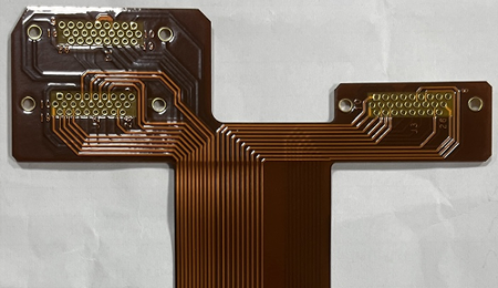
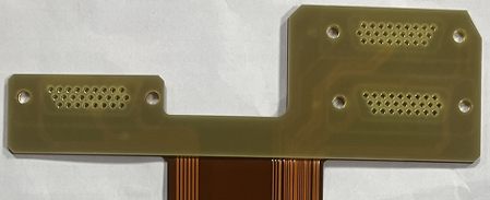
Recently, Best Technology faced a huge challenge in manufacturing 2oz copper rigid flexible PCB, this board looked simple in the picture but revealed many layers of technical challenges after entering mass production. But finally we finished this project very well and overcame these challenges, let’s see what the challenges of this project were and how our team overcame them!
Project Introduction
The board uses a 70/25 double-sided adhesive ED flexible substrate with a PI25/AD50 cover layer, plus a 2+2-layer dual-access structure that requires thick copper, small circular rings, tight clearance, and FR4 stiffeners with very limited clearance. Each of these parameters independently poses difficulties, but taken together, they require proper collaboration between engineering, fabrication, and process control.
This article explains:
- Why the design is inherently difficult
- What manufacturing risks exist
- How our engineering team solved each challenge
- What PCB designers should avoid in similar projects
- Why Best Technology can produce rigid-flex PCBs with high reliability
Material Structure and Key Design Parameters
The board consists of the following:
- Flexible substrate: double-sided adhesive ED copper 70/25
- Cover layer: PI 25 µm + Adhesive 50 µm
- Basic copper: 2 ounces copper
- Number of layers: Four-layer rigid-flex structure
- Critical routing: 0.15 mm minimum footprint/space
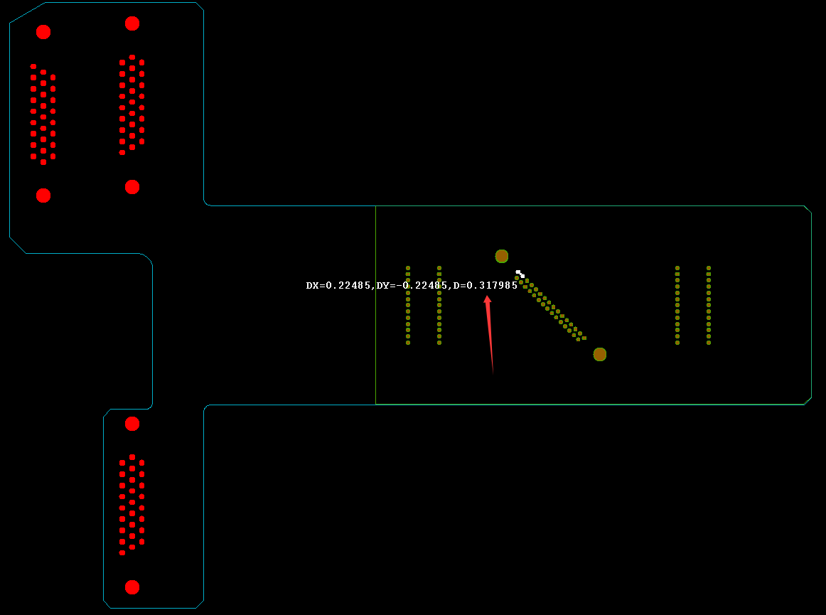
- Plated hole: 0.66 mm with hole spacing of only 0.60 mm
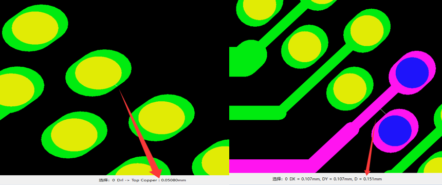
- Circular ring: 0.05 mm on certain bearings
- Stiffener: FR4 stiffener with 0.95 mm stiffener hole and 0.31 mm rib
This combination is common at advanced levels HDI rigid-flex PCB manufacturinghowever, its manufacturability is highly dependent on copper behavior, adhesive flow, and drilling tolerances.
Why Are These Rigid-Flex PCBs Basically Hard?
1. Thick copper increases the risk of side scratches
With 2 ounces of copper, the etching rate is higher and lateral etching—often called side etching—is more difficult to control. In this case, the amount of side etching reaches: 0.0070 ± 0.003 mm. For ultra-fine traces in a rigid-flex PCB designthis will eat into the design margin.
2. Small annular rings compromise through reliability
Bearings with 0.05 mm annular rings greatly limit drilling tolerances. In the Rigid and flexible PCB fabricationannular rings below 0.10 mm were classified as a high-risk feature.
3. Very tight stiffener clearance
Stiffeners required:
- Placement tolerance ±0.20 mm
- drilling tolerance ±0.05 mm
However, the designer only left a clearance of 0.15 mm, causing a mismatch between the two rigid-flex PCB stiffener alignment tolerances and actual manufacturing capabilities.
4. Thin FR4 stiffening ribs cause glue to overflow
Ribs that are only 0.31 mm wide cannot allow the adhesive to retreat during bonding, causing pure glue to overflow and block the stiffener holes.
Technical Challenge #1: Etching Thick Copper with Narrow Spacing
A 2 oz Thick copper PCB combined with:
- trace/spacing 0.15 mm
- circular ring 0.05 mm
- PTH 0.66mm
creating a situation where compensation is unavoidable.
However, after compensation (~0.007 mm), the remaining trace width drops to:
0.08mm (0.15 – 0.07mm)
This is below the range of safe manufacturing capabilities for most people rigid-flex PCB supplier.
Best Technology Solutions
- Eliminates compensation on the 0.15 mm trace
- Implement finely tuned etching controls
- Maintains final copper width ~0.10 mm
- Ensures full electrical reliability
This is a proven strategy advanced rigid-flex PCB manufacturing for thick copper buildings.
Technical Challenge #2: Annular Ring Integrity in Layered Holes
Annular rings <0.10 mm are particularly susceptible to:
- The drill wanders
- Etch the bottom
- Copper depletion
This is very important in Rigid-flex PCB with high reliabilitywhere integrity is paramount.
Best Technology Solutions
- Applying rigid board level PTH coating process
- Increased copper thickness inside the via barrel
- Drilling control is adjusted to 0.65±0.075mm
- Customer accepts partial ring damage as long as electrical integrity remains intact
This ensures consistent performance even in very dense rigid-flex PCB layouts.
Technical Challenge #3: Stiffer Bond, Alignment, and Adhesive Overflow
1. Why stiffener tolerance is problematic
In the rigid-flex PCB assemblyStiffeners are essential for mechanical reinforcement. However:
- The hole distance is only 0.60 mm
- Stiffener clearance is only 0.15 mm per side
- Combined tolerance ±0.25 mm
This inevitably causes the stiffener to cover the bearing unless advanced alignment controls are used.
2. Why does the glue overflow
The thin ribs (0.31 mm) cannot provide an outlet for the adhesive. During lamination:
- Glue goes into the hole
- The hole becomes clogged
- The board failed the inspection
3. Best Technology engineering solutions
- Pure adhesive that has been laminated to FR4 stiffener
- The stiffener holes are re-drilled after gluing
- Glue overflow is greatly reduced
- Added 100% AOI + manual inspection for hole cleaning
- Reject damaged boards, only send units that pass completely
This is a common best practice flexible PCB stiffener processing when tolerances are tight.
DFM Guidelines for Rigid-Flex PCB Designers
- Avoid rings under 0.15 mm, especially on 2-ounce copper rigid-flex PCB designs.
- Avoid combining thick copper with fine lines, this will increase production risks.
- Ensure stiffener clearance > total stack tolerance. If your clearance is less than the alignment tolerance, the stiffener will inevitably shift.
- Maintain stiffening ribs ≥0.5 mm
- Submit your design for DFM review before finalization. Good rigid-flex PCB manufacturer will help adjust piles, drill size, and stiffener layout to avoid costly redesigns.
This case shows how complicated it is Rigid-flex PCB—with 2 ounce copper, ultra-fine traces, small annular rings, and extreme stiffener limitations—can be successfully manufactured through detailed engineering, advanced process control, and disciplined quality screening.
Best Technology combines powerful fabrication capabilities with practical DFM insights, enabling customers to produce compact, reliable and manufacturable products rigid-flex PCB design who perform consistently under demanding conditions.
If you need support with your next rigid-flex or flexible PCB project, our technical team is ready to help with stack reviews, DFM checks, or test builds.
Tag: rigid flex PCB, Rigid Flex PCB Assembly, rigid flex PCB design, rigid flex PCB manufacturer, rigid flex PCB manufacturing
This entry was posted on Wednesday, December 31, 2025 at 18:23 and is filed under best PCB, best PCB, Design Guide, PCB News, Rigid Flex Circuits. You can follow any responses to this entry via the RSS 2.0 feed. You can skip to the end and leave a response. Ping is currently not allowed.
News
Berita Teknologi
Berita Olahraga
Sports news
sports
Motivation
football prediction
technology
Berita Technologi
Berita Terkini
Tempat Wisata
News Flash
Football
Gaming
Game News
Gamers
Jasa Artikel
Jasa Backlink
Agen234
Agen234
Agen234
Resep
Download Film
Gaming center adalah sebuah tempat atau fasilitas yang menyediakan berbagai perangkat dan layanan untuk bermain video game, baik di PC, konsol, maupun mesin arcade. Gaming center ini bisa dikunjungi oleh siapa saja yang ingin bermain game secara individu atau bersama teman-teman. Beberapa gaming center juga sering digunakan sebagai lokasi turnamen game atau esports.
Comments are closed, but trackbacks and pingbacks are open.