Why choose Low volume pcb? Let’s explore the meaning, benefits, applications, manufacturing and assembly processes, shipping time for low volume PCBs.
Are you having a problem with this problem?
- Waiting for 48 hours for offers?
- Forced to order 10 pcs when you need 2?
- Find a silent tweak in your Gerber file?
As a low volume PCB manufacturer, the best technology can provide you services and solutions:
- Ally Special Project – A Technical Contact Handling All 24/7 Needs, Eliminating Runaround Suppliers.
- Just order 1 board only for the material used ($ 0 regulatory fees), with details of real-time costs.
- Pre-production DFM Analysis-Eat feedback that can be followed up within 12 hours. Your design intention remains uncompromising.
Welcome to contact us if you have a low volume PCB request: sales@bestpcbs.com.
What does PCB mean low volume?
Low volume pcb Referring to the production model with a single number of orders usually ranging from 5 to 500 pieces, providing very flexible manufacturing services for R&D products, prototype validation, and small -scale test production. Unlike traditional mass production, it eliminates high printed costs and restrictions on minimum order quantity, allows fast design iterations (for example, design modifications within 48 hours), multi-process compatibility (for example, high frequency materials/HDI blind VIAS), and complex technical verification (EG, ± 5% Control impedance).
Why Choose a Low Volume PCB?
Low volume PCB advantages:
Lower face investment
- Avoid high tools and material deposits.
- Ideal for the R&D/Startup budget is limited.
Faster design iteration
- Receive prototypes in 72 hours (vs Week for traditional manufacturing).
- Test quickly and improve the design.
Flexibility for special requirements
- Supports niche material (ceramic pcb/flex).
- Accept the components provided by the customer.
Improved quality control
- 100% manual inspection per board.
- Capture defects before mass production.
Smooth market testing
- Launch Batch Pilot (100-500 units) for user validation.
- Customization of label/certification per region.
When to choose a low volume PCB board?
Low volume PCB board application:
- Devices that can be used smart: Smart Watch, AR/VR Glasses.
- Medical devices: Portable monitor, high precision surgical instrument.
- Industrial Control System: PLC Controller, Industrial Robot Core Council.
- BMS New Energy Vehicles: Battery management system.
- IoT Terminal: Smart meter, environmental monitoring node.
- Aerospace Special Circuit Board: Satellite control module, radar system.
- Consumer Electronics: Robot vacuum cleaners, smart door lock.
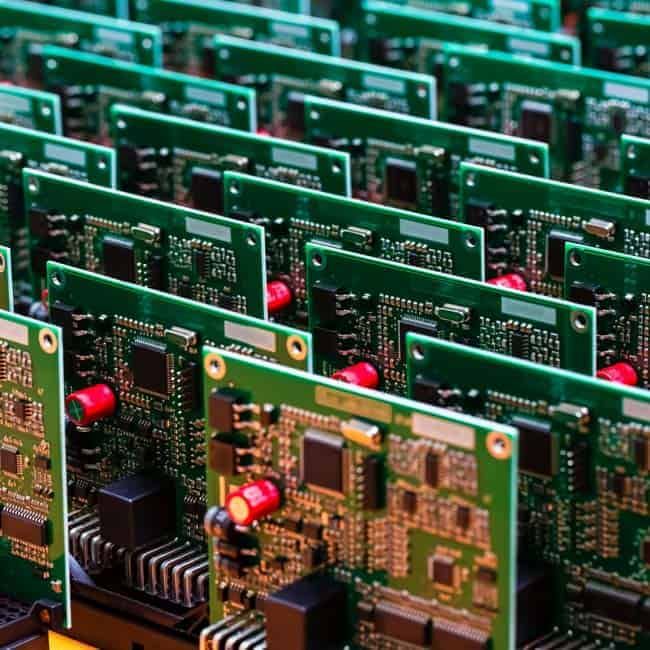
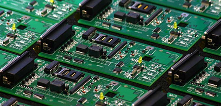
The process of making low volume pcb
1. Cutting Ingredients: Large large copper wrapped laminates are cut to design dimensions, support the production of small batch multi-varietas and minimize material waste.
2. Drilling: The CNC drilling machine makes it through a hole/VIAS blind/VIAS buried with the accuracy of ± 0.05mm hole position.
3. Metalization Hole: Chemical copper deposition + electroplating forms a conductive layer for electrical interconnection of layer board interlayer.
4. Dry film lamination: Photosensitive dry films are applied to the surface of the board as a mask base for pattern transfer.
5. Exposure to patterns: UV Exposure Machine transfers Gerber file patterns to dry films, forming resistant patterns.
6. ETSA PATTERN: Alkaline Eta Solutions Remove Unprotected Copper to form the right circuit pattern
Solder
7. Printing Mask: Liquid photosensitive soldder masks are applied and developed to form a permanent protective layer.
8. Surface Completed: IMMERSION GOLD/OSP/ENIG and other processes increase the reliability of polishing and corrosion resistance.
9. Machining Profile: CNC Milling/Laser Cutting allows the formation of irregular -shaped boards.
10. Electricity testing: Probe/Fixture Testing Flying Complete 100% Verification of Electric Performance, Ensuring No Shorts/Open.
11. Final Inspection: Visual Manual Inspection + AOI Optical Inspection Double Verification Appearance and Dimension Compliance.
12. Packaging & Delivery: Anti-static vacuum packaging + anti-gesting bearing material, a special label with a batch/serial number, an integrated logistics tracking system for full tracking

Low volume PCB assembly process
1. Component preparation: Sorting and checking the SMD/DIP components per bomb list, supporting the needs of a small batch multi-varietas with the ability to switching the material is fast.
2. Printing of Solder Pasta: Printing high precision stencils with a thickness control of ± 0.02mm for uniform soldering bearings.
3. Placement of SMD: Modular pick-and-plate machines allow high-speed micro component precision installation (chip 01005, BGA package).
4. Solder Reflow: Nitrogen Reflow Oven 10 Zone Achieved Lead Solder with a temperature precision ± 1 ° C for reliable connections.
5. Assembly through holes: Manual/automatic insertion machine handles components through holes, accommodating irregular shapes and precision placement.
6. Solder Selective: Local waves/solder selectively for the hole parts minimize thermal voltage while ensuring consistent connection quality.
7. Functional testing: The ICT/FCT system validates electricity performance, equipped with AOI/X-ray inspection for micro-default detection.
8. Conformal layer: Acrylic spray is applied per requirement to increase moisture/dust/corrosion resistance.
9. Packaging & Delivery: Special anti-static packaging with bearing materials, integrated logistics tracking for safe delivery and can be tracked.
Why choose the best technology as a low volume PCB manufacturer?
The reason why choosing us as Low volume PCB manufacturer:
- One Roof Solution: Full link services that include PCB design for assembly, eliminating the client’s need to coordinate with many suppliers. Reducing the R&D cycle by more than 30% and decreases cross -departmental communication costs.
- Optimization of Free DFM Design: The 19 -year -old technical team provides design analysis for manufacturing (DFM) to identify earlier design weaknesses, minimize subsequent modification costs, increase the success rate of the first board by 40%, and avoid re -work losses in mass production.
- Accumulation of 19 years of experience: Focusing on low volume PCB production, serving more than 2,000 clients. The database of a rich process allows fast adaptation to complex process requirements, ensuring increased efficiency and production results.
- Four -layer quality control system: Incoming material inspection, patrol inspection in process, 100%final product inspection, and reliability testing. Achieve a batch inspection full of defects below 0.3%, significantly outperformed the average industry and ensure product reliability.
- Dynamic Cost Optimization Solution: Cost reduction strategies adjusted based on the client’s budget, including material substitution, process adjustment, and batch collection. Reducing costs by 15% -30% while maintaining quality, maximizing cost effectiveness.
- Fast Prototype 24 Hours: Prototyping that is accelerated 24 hours for a two-sided board, shipping 3 days for 4-6 layers boards, 50% faster than conventional schedules. Speed up design validation and market entry.
- Flexible production scheduling: Special production lines support small batch orders starting from 50 pieces. The intelligent scheduling system allows changes in fast paths (under 2 hours), flexibly accommodating the needs of multi-commercial and multi-match production.
- Professional Assembly Support: Comprehensive assembly services include SMT placement, DIP insertion, and conformal layer. Combined with the right solder temperature curve control and soldering connection inspection, ensuring the accuracy of component assembly ± 0.025mm and stable electricity performance.
Waiting time for our low volume PCB
Waiting time for 1-50 pieces
| Layer | Normal service | The fastest service |
| 1 | 7 days | 24 hours |
| 2 | 8 days | 24 hours |
| 4 | 10 days | 48 h |
| 6 | 10 days | 72 h |
| 8 | 12 days | 72 h |
| ≥10 | TBD | TBD |
Waiting time for 50-500 pieces
| Layer | Normal service | Accelerated service |
| 1 | 4-6 days | 2-3 days |
| 2 | 5-8 days | 2-3 days |
| 4 | 8-12 days | 3-5 days |
| 6 | 8-12 days | 4-6 days |
| 8 | 12-16 days | 6-8 days |
| ≥10 | 18-20 days | TBD |
How do you get an offer for a low volume PCB project?
Check list of important bid submissions for low volume PCB projects
- Design data: Complete Gerber File (274x, NC Drill) with special details of the layer (dimensions, thickness of copper, through specifications).
- Bomb: List of detailed components with section number, producer, number, and critical component flag.
- Technical Specifications: The number of PCB layers, material types (for example, FR4, high TG), surface finish (Enig/Hasl/OSP), target impedance, and special processes (HDI, Blind Vias).
- Quantity & Time Line: Annual volume/batch and required shipping date (prototype for mass production).
- Quality standards: Compliance with IPC-A-600/A-610, reliability test (thermal cycling, vibration), and certification (Rohs, UL).
- Assembly requirements (if applicable): Specifications of SMT/DIP, Type of Solder Pasta, Test Protocol (ICT/FCT), and Coating Requirements.
Welcome to contact us if you have questions for low volume PCB design, manufacturing, assembly: sales@bestpcbs.com.
Tags: low volume PCB, low volume PCB assembly, low volume PCB manufacturer
This entry was posted on Thursday, September 18, 2025 at 18:10 and was submitted under the best PCB, BestTPCB, FR4 PCB. You can follow any response to this entry through RSS 2.0 bait. You can jump to the end and leave a response. Pinging is currently not permitted.
News
Berita
News Flash
Blog
Technology
Sports
Sport
Football
Tips
Finance
Berita Terkini
Berita Terbaru
Berita Kekinian
News
Berita Terkini
Olahraga
Pasang Internet Myrepublic
Jasa Import China
Jasa Import Door to Door
Comments are closed, but trackbacks and pingbacks are open.