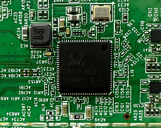
A QFN packageshort for Quad Flat Unleadedis a surface-mount integrated circuit package designed for compact layout and efficient electrical performance. The term Meaning of QFN refers to a square or rectangular IC package that uses exposed copper pads instead of protruding wires for electrical connections.
Due to their low profile and short signal path, QFNs have become the preferred choice in modern electronics where space efficiency and signal integrity are paramount.
What does QFN stand for?
A QFN package (Quad Flat No-Lead) is a surface-mounted IC package with exposed pads on the bottom instead of protruding wires. Electrical connections are made via metal terminations located on the bottom perimeter of the package, often combined with an exposed thermal pad in the center.
From a manufacturing point of view, QFN the package reduces parasitic inductance and resistance while enabling compact PCB layouts. This is why they are widely used in RF devices, power management ICs, microcontrollers, and high-speed digital components.
Key structural characteristics include:
- Flat body profile and no lead
- Bottom side copper pad for electrical connection
- Optional open pads for thermal and ground connections
- Compatibility with standard SMT reflow processes
QFN Package Type
QFN packages are available in several structural variations to meet different thermal, mechanical and manufacturing needs.
Common types include:
- Standard QFN – Leadless flat design with perimeter padding and optional exposed thermal pads
- Wettable Side QFN – Modified sidewalls so solder fillets are visible for AOI inspection
- Double Row QFN – Two rows of bearings to support higher pin counts
- QFN Air Cavity – Used in RF and microwave designs to reduce dielectric loss
- QFN Pull Back – Pads are slightly recessed inward to increase solder joint reliability
Each QFN package type balances solderability, inspectability, and electrical performance differently, which directly impacts PCB assembly strategies.
QFN Package Benefits
The popularity of QFN packages is driven by several clear technical advantages.
Key benefits include:
- Smaller footprint compared to QFP and other leaded packages
- Outstanding thermal performance through the open center bearing
- Low electrical parasitesimprove signal integrity
- Improved mechanical stability due to the large solder contact area
- Reduce EMIespecially in high frequency designs
For dense layouts and performance-critical circuits, QFNs often provide measurable advantages over traditional packages.
Disadvantages of QFN Packages
Despite their advantages, QFN packages also introduce specific manufacturing challenges that must be overcome during design and assembly.
Limitations include:
- Difficult visual inspection because the joints are hidden underneath
- Higher assembly sensitivity for stencil design and reflow profiles
- Complexity of reworkespecially for the middle thermal pad
- Less forgiving of PCB flatness issues
These drawbacks do not make QFN inferior, but require tighter process control compared to superior alternatives.
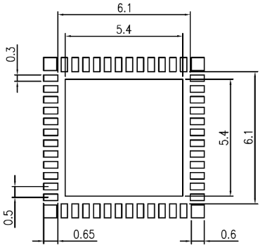
QFN Packet Size
QFN package sizes are standardized based on body dimensions, pin count, and pad spacing, allowing designers to balance I/O density, thermal performance, and routing complexity. Although QFN packages are often described simply as “small” or “compact,” the range of available sizes is much wider than many engineers expect.
General Standard QFN Body Sizes
The following QFN package sizes are widely used in consumer, industrial and automotive electronic devices:
- 2 × 2 mm – Ultra-compact sensor, low power analog IC
- 3 × 3 mm – LDO, small MCU, interface IC
- 4×4 mm – Mixed signal IC, power management device
- 5×5mm – MCU, RF transceiver, motor driver
- 6×6 mm – Connectivity chips, signal processors
- 7×7mm – High pin count controllers, automotive ICs
- 8×8mm – Power IC with increased thermal requirements
- 10×10mm – High density logic, network IC
- 12 × 12 mm and larger – RF front end, industrial control IC
This size is usually specified as body size × body sizedoes not include solder fillets.
QFN Package Size based on Number of Pins
Pin count scales with package size and pad spacing. Common configurations include:
- 8–16 pins – 2 × 2 mm to 3 × 3 mm
- 20–32 pins – 4 × 4 mm to 5 × 5 mm
- 40–64 pins – 6×6mm to 7×7mm
- 64–100+ pins – 8 × 8 mm to 10 × 10 mm and above
Higher pin counts are often used Double row QFN designed to maintain reasonable pad tone while increasing I/O density.
Distinctive QFN Pad Tone Options
Pad pitch directly affects PCB routing and soldering tolerance:
- 0.4mm – Very smooth tone, HDI recommended
- 0.5mm – Common for compact QFN packages
- 0.65mm – Easier routing and assembly
- 0.8mm – Larger QFN format with higher power handling
Pad tones typically range from 0.4mm to 0.65mmwhich directly affects stencil thickness, solder paste selection, and placement accuracy.
How to Solder a QFN Package on a PCB?
Soldering QFN packages requires a controlled SMT process rather than manual techniques.
Standard workflow includes:
1. Solder paste printing using precisely designed stencils
2. Accurate pick-and-place alignment with vision correction
3. Reflow soldering using a controlled temperature profile
4. Post-reflow inspectionusually X-ray rather than AOI
Hand soldering is generally impractical for QFNs because of the hidden pads and the thermal mass of the exposed center pad.
Key Considerations in Soldering QFN Packages
- The pad design should match the pitch of the QFN, with open pads extending 0–0.15 mm and 40–60% through openings to balance solder volume and heat dissipation.
- Humidity control requires pre-baking QFN components (e.g., 125 °C for 4 h) to avoid popcorn defects during reflow.
- Stencil thickness and opening design should be optimized (≤0.12 mm, segmented thermal pad opening) to improve paste release and reduce voids.
- Reflow profiling must tightly control ramp rate, soak time, and peak temperature to achieve complete solder activation without floating components.
- Manual soldering, if necessary, should use flux-assisted hot air heating with uniform thermal distribution to avoid local damage.
- Inspection methods should combine edge wetting inspection with X-ray analysis to identify solder defects hidden beneath the packaging.
How Are QFN Packages Created?
The process of creating QFN packages is different from leaded packages such as QFP.
General steps include:
- Stamp or etch the lead frame
- Die attach to the exposed thermal pad
- Wire ties to perimeter pads
- Mold encapsulation
- Singulation into individual packages
Because the package relies on a main frame and not on molded leads, the result is a compact, mechanically robust IC with excellent thermal conduction pathways.
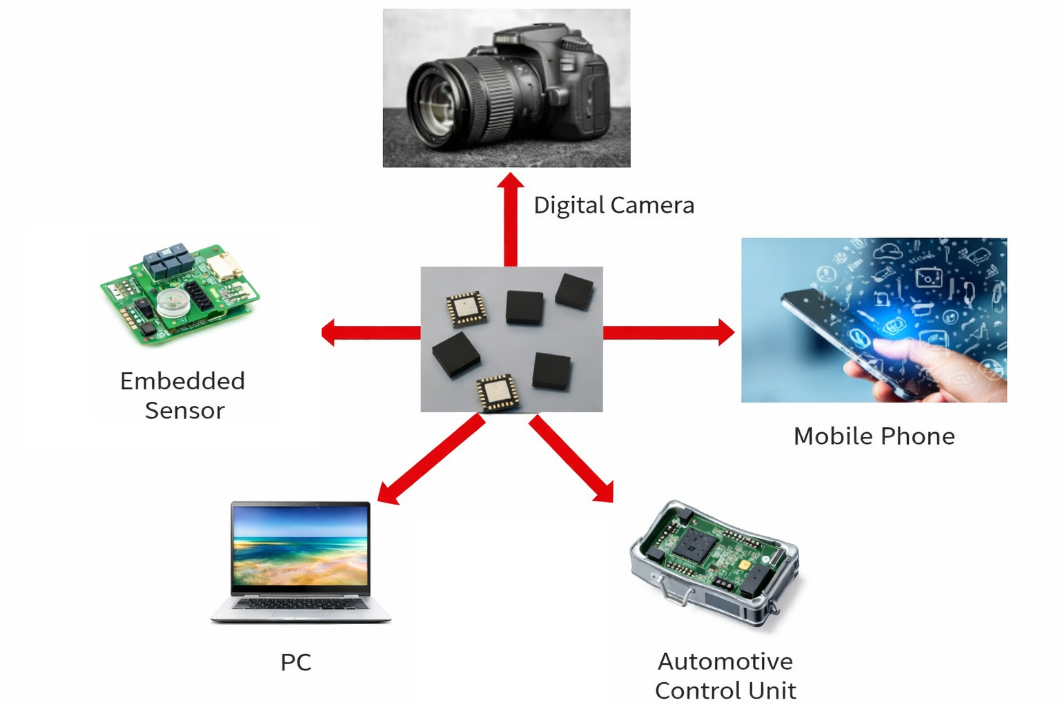
QFN Package Application
QFN packages are widely adopted in various industries that demand compact form factors and stable electrical behavior.
Typical applications include:
- Consumer electronics and wearable devices
- RF and wireless communication modules
- Automotive control unit
- Power management IC
- Embedded industrial sensors and controllers
In many of these applications, QFN replaces QFP specifically to reduce board area and increase performance margins.
What Is a QFP Plan and How Are They Structurally Different?
A MFF (Quad Flat Pack) uses gull wing tips that extend out from all four sides of the pack body. These visible clues make inspection easier, but also lead to longer electrical paths and larger footprints.
When MFF packages once dominant in microcontrollers and ASICs, their size and lead geometry limit their usefulness in modern compact designs.
Structurally, a MFF package features:
- Outward clues are visible all around
- Larger pad spacing on PCB
- Easier manual soldering and optical inspection
- Increased susceptibility to lead damage during handling
What is the Difference Between QFN and QFP?
That QFN vs QFP comparison is one of the most common questions during IC selection.
Key differences include:
| Aspect | QFN | MFF |
| Lead | There are no external clues | Seagull wings lead |
| Footprint | Smaller | Bigger |
| Thermal performance | Very good | Currently |
| Inspection | X-rays are required | Visual AOI possible |
| Assembly tolerance | Tighter | Be more forgiving |
QFP remains attractive for prototypes and low-complexity designs, while QFN is preferred in production-grade electronic devices with limited space.
How to Choose the Right IC for Your PCB?
The choice between a QFN package and a QFP package depends on practical design priorities and not on mere preference.
Consider QFN if:
- Limited PCB space
- Heat dissipation is very important
- High-speed or RF signals are involved
Consider QFP if:
- Easy inspection and rework required
- Limited assembly capabilities
- The design is still in the early prototype stage
Matching the package type to your production maturity is often more important than theoretical performance advantages.
General Questions
1. What is meant by QFN in the field of electronics?
QFN means Quad Flat Unleadedrefers to an IC package with bottom side pads and no protruding wires.
2. Is QFN better than QFP?
QFN is not universally better, but offers superior size efficiency and thermal performance compared to QFP.
3. Can QFN be soldered by hand?
In most cases, no. QFN requires reflow soldering for reliable results.
4. Why does QFN require X-ray examination?
Because the solder joints are hidden beneath the packaging, visual inspection cannot be performed.
5. What surface finish is most suitable for QFN?
ENIG and OSP are commonly used because of their flatness and solderability.
Tags: qfn, qfn meaning, qfn package size, qfn package, qfn vs qfp, qfn package types
This entry was posted on Monday, January 12, 2026 at 18:30 and is filed under best PCB, best PCB, FAQ, PCBA. You can follow any responses to this entry via the RSS 2.0 feed. You can skip to the end and leave a response. Ping is currently not allowed.
News
Berita Teknologi
Berita Olahraga
Sports news
sports
Motivation
football prediction
technology
Berita Technologi
Berita Terkini
Tempat Wisata
News Flash
Football
Gaming
Game News
Gamers
Jasa Artikel
Jasa Backlink
Agen234
Agen234
Agen234
Resep
Download Film
Gaming center adalah sebuah tempat atau fasilitas yang menyediakan berbagai perangkat dan layanan untuk bermain video game, baik di PC, konsol, maupun mesin arcade. Gaming center ini bisa dikunjungi oleh siapa saja yang ingin bermain game secara individu atau bersama teman-teman. Beberapa gaming center juga sering digunakan sebagai lokasi turnamen game atau esports.
Comments are closed, but trackbacks and pingbacks are open.