Poor PCB stackup decisions can introduce signal integrity issues that only become visible during testing or, worse, after deployment. In high-speed electronics, these problems are rarely isolated. They are usually tied to how layers were arranged, how materials were selected and how closely the design aligned with manufacturing realities.
Stackup design sits at the centre of signal behaviour, EMI control and long-term reliability. It defines how signals travel, how return paths behave and how consistently impedance can be maintained across the board. In multilayer designs, even small variations in spacing or material properties can create instability that is difficult to trace later.
For engineering teams, the challenge is not understanding signal integrity theory, it is applying it in a way that works in production. Manufacturing tolerances, material availability and assembly constraints all influence whether a theoretically sound design performs as expected.
This article explains how PCB stackups affect signal integrity in high-speed electronics, with a focus on practical engineering decisions and manufacturable outcomes.
PCB Stackups in High Speed Electronics
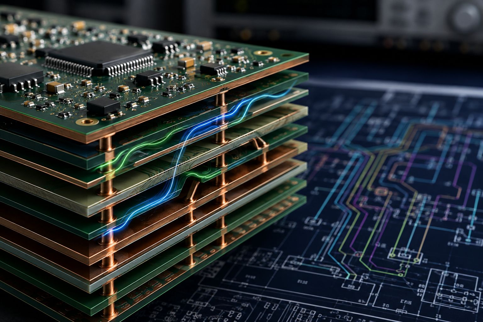
PCB stackups define how conductive and insulating layers are arranged within a board, directly affecting signal integrity, EMI and manufacturability.
In high-speed electronics, this structure determines how signals interact with reference planes, how electromagnetic fields are contained and how impedance can be consistently maintained across the design. A multilayer stackup is not just a vertical arrangement of copper and dielectric. It is a controlled electrical environment where spacing, symmetry and material behaviour all influence performance.
For example, placing high-speed signal layers adjacent to continuous ground planes creates predictable return paths and reduces noise. If those relationships are poorly defined, signal reflections and interference become more likely. This is particularly important in designs handling fast data transmission, where even small inconsistencies can affect timing margins.
From a manufacturing perspective, each layer added increases complexity. Lamination cycles, material selection and thickness control must all be tightly managed. Variations in dielectric thickness or copper distribution can shift impedance and introduce performance variation between production runs.
Effective stackup design, therefore, requires early alignment between engineering intent and manufacturing capability. Without this, designs that perform well in simulation can struggle to deliver consistent results in production.
Scale Your Production
From prototype to full-scale electronic assembly, our UK facility is equipped to handle your requirements.
Get a Quote
Signal Loss Across PCB Layers
Signals lose strength as they travel across PCB layers due to resistance, dielectric loss and routing complexity.
In high-speed PCB designs, signal loss becomes more pronounced as frequency increases. Conductor loss occurs as current flows through copper traces, where surface roughness and skin effect increase resistance at higher frequencies. At the same time, dielectric loss arises as electromagnetic energy is absorbed by the insulating material between layers, reducing signal amplitude as it propagates.
Routing decisions amplify these effects. Long trace lengths increase exposure to both conductor and dielectric losses, while unnecessary layer transitions introduce vias that disrupt signal continuity. Each via creates a local impedance change, which can lead to reflections and additional insertion loss if not carefully controlled.
A practical example is a high-speed interface routed across multiple layers to navigate a dense layout. If the routing path includes excessive vias and inconsistent reference planes, signal degradation can accumulate across the path. This can reduce signal clarity and introduce timing uncertainty.
From a manufacturing standpoint, material consistency and process control are critical. Variations in dielectric thickness, resin content or copper profile can increase loss beyond design expectations, leading to performance variation between boards.
Impedance Control and Layer Configuration
Controlled impedance depends heavily on accurate layer configuration, spacing and dielectric consistency within the PCB stackup.
In high-speed PCB design, impedance defines how signals propagate along traces. It is influenced by trace width, copper thickness, dielectric height and the proximity of reference planes. These factors must remain consistent across the board to prevent reflections, signal distortion and timing errors.
Layer configuration plays a central role in maintaining this consistency. Signal layers positioned close to solid ground planes create stable impedance conditions, while uneven spacing or inconsistent dielectric materials can introduce variation. Even small deviations in layer thickness can shift impedance outside acceptable ranges for high-speed interfaces.
A practical example is differential pair routing in communication systems. These signals rely on tightly controlled spacing and symmetry. If the dielectric layer between the signal and reference plane varies during fabrication, impedance imbalance can occur, leading to skew and reduced signal integrity.
From a manufacturing perspective, achieving controlled impedance requires precise process control. Etching tolerances, material selection and lamination accuracy all influence the outcome. Designs must reflect these realities to ensure impedance targets are achievable and repeatable in production.
Engineering-Led Solutions
Work with a team that understands modern electronics and end-to-end manufacturing.
Our Expertise
Ground Planes and Signal Stability
Well-designed ground planes improve signal stability by reducing noise, minimising EMI and providing reliable return paths.
In high-speed PCB designs, signals do not travel in isolation. Every signal requires a return path, and this path typically follows the nearest reference plane. A continuous ground plane provides a low-impedance route for return currents, keeping signal loops compact and reducing susceptibility to interference.
When ground planes are poorly implemented, signal behaviour becomes less predictable. Gaps, splits or interruptions in the plane force return currents to detour around discontinuities. This increases loop area, which raises the risk of radiated emissions and noise coupling into adjacent traces.
A common failure scenario involves signals crossing a split in the ground plane. Even if the signal trace itself appears correctly routed, the disrupted return path can introduce instability, reflections and increased EMI. These issues are difficult to diagnose once the board is assembled.
Maintaining continuous ground planes and placing them close to signal layers helps stabilise signal behaviour. This approach also supports EMI control by containing electromagnetic fields within defined layers. This becomes particularly important during multilayer PCB assembly, where alignment accuracy and layer integrity directly influence grounding performance.
From a manufacturing perspective, maintaining ground plane integrity requires precise layer alignment and consistent lamination. Any misregistration or variation in copper distribution can affect how effectively the plane supports signal return paths. Stable grounding depends on both sound design and controlled fabrication processes.
Cross Talk Between High Speed Signals
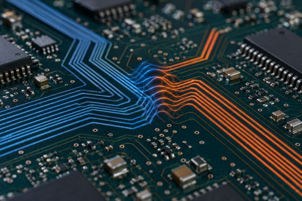
Crosstalk occurs when high-speed signals interfere with adjacent traces, potentially causing timing and reliability problems.
In high-speed PCB environments, signals generate electromagnetic fields as they propagate along traces. When traces are routed too closely or run in parallel over extended distances, these fields can couple into neighbouring signals. This interaction introduces unwanted noise, which can distort signal edges and affect timing accuracy.
The risk increases in dense multilayer designs where routing space is limited. High-speed interfaces, particularly those operating with fast rise times, are more sensitive to coupling effects. Even where signal integrity appears acceptable in isolation, adjacent activity can introduce intermittent issues under real operating conditions.
A common example is a tightly packed routing channel where multiple high-speed lines run in parallel without sufficient spacing or shielding. In this scenario, one signal switching state can induce voltage changes in a neighbouring trace, leading to data errors or reduced noise margins.
Mitigation requires careful stackup planning and routing discipline. Increasing trace spacing, introducing ground shielding and maintaining consistent reference planes all help reduce coupling. These measures must be balanced against board size, layer count and manufacturing constraints to ensure a practical and producible design.
Ready to start your project?
Contact our technical team today to see how Altimex can streamline your electronics supply chain.
Contact Us
Electromagnetic Interference in PCB Design
PCB stackup design plays a major role in controlling electromagnetic interference and reducing unwanted emissions.
In high-speed electronics, signals switching at fast rates generate electromagnetic fields that can radiate beyond their intended paths. If these fields are not properly contained within the PCB structure, they can interfere with nearby circuits or external systems, leading to compliance issues and unstable performance.
Stackup configuration directly influences how effectively these fields are controlled. Placing signal layers between continuous ground or power planes helps confine electromagnetic energy, reducing radiation. This approach creates a controlled environment where fields are absorbed or redirected within the board rather than escaping into surrounding space.
Problems arise when stackups lack proper shielding or when reference planes are inconsistent. Gaps in grounding, poorly positioned signal layers or excessive layer transitions can allow fields to spread, increasing the risk of interference.
A practical scenario involves industrial electronics operating in electrically noisy environments. Without a well-structured stackup, external noise can couple into signal paths, degrading performance.
Manufacturing consistency is critical. Variations in layer spacing or material properties can alter electromagnetic behaviour, making EMI performance difficult to predict across production batches.
Dielectric Materials and Signal Performance
Dielectric material selection affects signal speed, impedance consistency and electrical losses within high-speed PCBs.
In a multilayer stackup, dielectric materials sit between conductive layers and directly influence how signals propagate. The dielectric constant determines signal velocity, while loss characteristics affect how much energy is absorbed as signals travel through the board. In high-speed designs, even small variations in these properties can alter signal timing and reduce overall integrity.
Standard FR4 is widely used due to cost and availability, although its electrical performance can vary with frequency and temperature. At higher data rates, this variability can lead to inconsistent impedance and increased signal loss. For applications requiring tighter control, low-loss laminates provide more stable dielectric properties, supporting predictable signal behaviour across operating conditions.
Material choice also affects manufacturability. Specialist laminates may require different processing conditions, tighter handling controls and longer lead times. If these constraints are not considered during design, production delays or inconsistencies can occur.
A practical example is a high-frequency board designed using standard materials without accounting for dielectric variation. While initial testing may appear acceptable, performance can shift across production batches. Selecting appropriate materials early helps ensure both electrical stability and reliable manufacturing outcomes.
Trace Routing Across PCB Stackups
Effective trace routing reduces signal degradation by controlling spacing, layer transitions and return path continuity.
Routing decisions define how signals interact with the stackup in practice. Even a well-designed layer structure can underperform if routing introduces unnecessary complexity. Long trace lengths increase exposure to loss mechanisms, while excessive vias introduce impedance discontinuities and potential reflection points.
Maintaining consistent reference planes during routing is critical. Signals should remain adjacent to a continuous ground plane wherever possible, ensuring stable return paths. When signals transition between layers, the associated return path must also be preserved. If this continuity is broken, signal loops expand and noise susceptibility increases.
A common issue arises in dense designs where routing constraints force signals across multiple layers without maintaining consistent reference conditions. This can lead to impedance variation and reduced signal quality, particularly in high-speed interfaces.
From a manufacturing perspective, routing must remain practical. Tight spacing, complex via structures and aggressive layer usage can reduce fabrication yield or introduce variability. Designers must balance electrical performance with manufacturability, ensuring routing strategies support both signal integrity and consistent production outcomes.
PCB Thickness and Electrical Performance
PCB thickness influences impedance, mechanical stability and thermal performance in high-speed electronic systems.
In stackup design, overall thickness determines the spacing between signal layers and reference planes, which directly affects impedance control. Thicker boards increase this distance, making it harder to maintain tight impedance targets required for high-speed signals. Thinner constructions allow closer layer coupling, supporting more consistent electrical behaviour, although they demand tighter manufacturing tolerances.
Mechanical considerations also play a role. Thicker PCBs provide rigidity, which can be beneficial for larger assemblies or connectors under stress. Thinner boards, while electrically advantageous, can introduce handling challenges during fabrication and assembly.
From a manufacturing perspective, maintaining uniform thickness across multilayer builds is critical. Variations in lamination pressure or material distribution can lead to inconsistent electrical performance between boards. Balancing thickness with both electrical and production requirements is essential for reliable high-speed designs.
Thermal Performance in High Speed PCBs
High-speed electronics generate thermal loads that can affect signal integrity, reliability and long-term PCB stability.
As operating speeds increase, power density within components and traces rises, leading to concentrated heat within the PCB structure. Elevated temperatures can alter dielectric properties, shifting impedance and affecting signal propagation. Over time, thermal stress can also impact material stability, leading to reliability concerns.
Stackup design influences how heat is distributed and managed. Balanced copper layers help spread thermal energy across the board, reducing localised hotspots. Thermal vias provide vertical heat transfer paths, improving dissipation through the stackup.
A practical scenario involves dense processing hardware where uneven heat distribution creates stress between layers. This can affect both electrical performance and structural integrity.
From a manufacturing perspective, consistent material selection and controlled lamination are essential. Variations in copper distribution or layer bonding can reduce thermal efficiency and introduce performance variation across production batches.
Manufacturing Support for High Speed PCB Projects
High-speed PCB projects benefit from early collaboration between engineers and manufacturers to reduce production risks and improve reliability.
Stackup design decisions made in isolation can lead to challenges during fabrication and assembly. Manufacturing teams provide insight into achievable tolerances, material behaviour and process limitations.
Early design-for-manufacture input allows potential issues to be identified before production begins. This includes validating stackup configurations, confirming material availability and ensuring impedance targets align with fabrication capabilities.
A typical scenario involves a design requiring tight impedance control across multiple layers. Without manufacturing input, the design may rely on assumptions that are difficult to achieve consistently. Early collaboration helps refine the stackup to match real production conditions.
For engineering teams developing high-speed PCB designs, aligning performance requirements with manufacturability is critical. If you need support reviewing stackup design or production feasibility, you can contact us to discuss suitable manufacturing and assembly approaches.
PakarPBN
A Private Blog Network (PBN) is a collection of websites that are controlled by a single individual or organization and used primarily to build backlinks to a “money site” in order to influence its ranking in search engines such as Google. The core idea behind a PBN is based on the importance of backlinks in Google’s ranking algorithm. Since Google views backlinks as signals of authority and trust, some website owners attempt to artificially create these signals through a controlled network of sites.
In a typical PBN setup, the owner acquires expired or aged domains that already have existing authority, backlinks, and history. These domains are rebuilt with new content and hosted separately, often using different IP addresses, hosting providers, themes, and ownership details to make them appear unrelated. Within the content published on these sites, links are strategically placed that point to the main website the owner wants to rank higher. By doing this, the owner attempts to pass link equity (also known as “link juice”) from the PBN sites to the target website.
The purpose of a PBN is to give the impression that the target website is naturally earning links from multiple independent sources. If done effectively, this can temporarily improve keyword rankings, increase organic visibility, and drive more traffic from search results.
Comments are closed, but trackbacks and pingbacks are open.