A breakout board is a small printed circuit board that makes an electronic component easier to use, test, and connect. Many modern chips, sensors, connectors, and modules use tiny packages or dense pin spacing that are not friendly for hand wiring, breadboard experiments, or fast prototyping. A breakout board solves this problem by “breaking out” those small or hard-to-access pins into larger pads, pin headers, screw terminals, or standard connectors.
What is a Breakout Board?
A breakout board is a PCB that takes the electrical pins of a component and routes them to easier connection points. The component may be a sensor IC, power chip, communication module, connector, USB interface, ESP32 module, or any other part that needs a more practical interface. In simple terms, a breakout board acts as a bridge between a tiny electronic component and a user-friendly circuit environment.
For example, a small surface-mount IC may have pins spaced only 0.5 mm apart. That is difficult to solder by hand and impossible to place directly into a breadboard. A breakout board mounts that IC on a small PCB and routes each pin to 2.54 mm headers, test pads, or terminal blocks. This makes the component much easier to connect with jumper wires, breadboards, test equipment, or another PCB.
A typical breakout board may include:
- The main chip, module, sensor, or connector
- Pin headers or solder pads
- Power and ground pins
- Pull-up or pull-down resistors
- Decoupling capacitors
- Voltage regulator or level shifting circuit
- Labels printed on the silkscreen
- Mounting holes for mechanical installation
What is a Breakout Board?
What is a Breakout in Electrical Terms?
In electrical and electronic design, breakout means extending or separating multiple electrical signals from a compact source into more accessible connection points.
The source may be:
- A fine-pitch IC package
- A board-to-board connector
- A cable connector
- A USB port
- A camera module connector
- A microcontroller module
- A sensor package
- A test fixture interface
The “breakout” process makes each signal easier to identify, probe, solder, or connect. This is why breakout boards are common in laboratories, repair shops, embedded system development, and PCB prototyping.
In PCB development, breakout can also describe the routing area where traces leave a dense component footprint. For example, when routing a BGA package assembly, engineers may talk about “BGA breakout routing,” which means fan-out routing from the BGA pads to other PCB layers.
Is a Breakout Board a PCB?
Yes, in most cases, a breakout board is a type of PCB. More specifically, it is a small functional PCB designed to expose signals from one component, connector, or module.
A breakout board PCB is usually simpler than a full product PCB. It may not contain a complete system. Instead, it focuses on making one part easier to connect and test.
A breakout board can be used alone, connected to a breadboard, plugged into a development board, or integrated into a larger test fixture. In professional engineering workflows, breakout boards are often used before the final PCB design is completed.
What is the Purpose of a Breakout Board?
The main purpose of a breakout board is to make an electronic component easier to connect, evaluate, and integrate. It reduces the gap between the small physical structure of modern electronics and the practical needs of engineers during development.
1. Easier prototyping
Many ICs and modules are not breadboard-friendly. A breakout board converts small pins into larger headers or pads, allowing fast connection with jumper wires, test clips, or soldered leads.
2. Faster component testing
Before using a new sensor, power IC, connector, or communication chip in a product, engineers often need to check whether it performs as expected. A breakout board provides a convenient test platform.
3. Better access to signals
Breakout boards make signals easier to probe with an oscilloscope, multimeter, logic analyzer, or functional test fixture. This is especially useful during debugging.
4. Reduced soldering difficulty
Fine-pitch SMD parts can be hard to solder manually. A breakout board allows the difficult component to be mounted once, while the user connects to larger and more forgiving pads.
5. Easier system integration
A breakout board can help connect a small module to another system, such as an Arduino, Raspberry Pi, ESP32, industrial controller, or custom test board.
6. Safer development
Some breakout boards include basic protection, such as reverse polarity protection, ESD protection, current-limiting resistors, or level shifting.
Types of Breakout Boards
Breakout boards come in many forms because electronic components have different electrical and mechanical needs. Below are common types used in prototyping and PCB design.
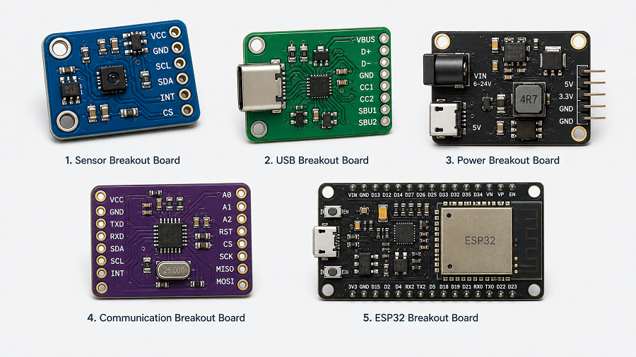
1. Sensor Breakout Board
Sensor breakout boards are very popular in embedded systems. They may include temperature sensors, pressure sensors, motion sensors, light sensors, gas sensors, current sensors, or magnetic sensors.
Many sensor ICs use small packages and require supporting parts such as pull-up resistors or capacitors. A breakout board places those parts on the PCB and provides pins for power, ground, and signal communication.
Common interfaces include I2C, SPI, UART, analog output, and digital output.
2. Microcontroller Breakout Board
A microcontroller breakout board exposes the pins of a microcontroller or module. It may support ESP32, STM32, RP2040, ATmega, or other MCU families.
A breakout board for ESP32 is especially useful because ESP32 modules include Wi-Fi, Bluetooth, GPIO, ADC, UART, SPI, I2C, PWM, and power pins. A breakout board helps organize those pins into a more usable layout.
3. Connector Breakout Board
Connector breakout boards expose small or dense connectors to larger pads or headers. Common examples include USB, HDMI, FFC/FPC, RJ45, SD card, SIM card, and board-to-board connectors.
4. Power Breakout Board
Power breakout boards help distribute or adapt power. They may include voltage regulators, screw terminals, fuses, current sense resistors, reverse polarity protection, or DC jack connectors.
They are often used in robotics, LED control, battery systems, and industrial prototypes.
5. Communication Breakout Board
These boards provide access to communication chips or modules, such as RS485, CAN, Ethernet, LoRa, Wi-Fi, Bluetooth, NFC, or USB-to-UART converters.
6. IC Adapter Breakout Board
An IC adapter breakout board converts one package style into another more usable form. For example, it may convert SOP, QFN, TSSOP, MSOP, or DFN packages to DIP-style headers.
Breakout Board vs Breadboard
The topic of breakout board vs breadboard is common because both are used in prototyping. However, they are not the same.
A breadboard is a solderless platform used to build temporary circuits. A breakout board is a PCB that makes a specific component easier to connect.
A breakout board and a breadboard are often used together. For example, a small sensor breakout board can plug into a breadboard, allowing the user to build a temporary circuit around it.
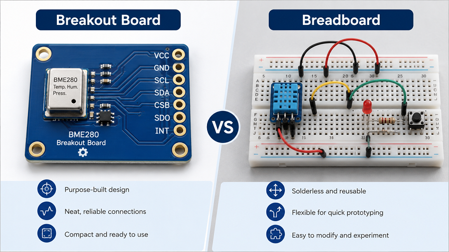
However, for high-speed signals, RF circuits, precision analog circuits, USB, CAN, or power electronics, a breadboard may create poor results due to parasitic capacitance, loose contacts, and uncontrolled wiring. In those cases, a breakout board or custom PCB is a better choice. Here is a detailed comparison between them:
| Comparison Point | Breakout Board | Breadboard |
|---|---|---|
| Structure | Custom PCB with routed traces | Solderless plastic board with internal metal clips |
| Main purpose | Expose component pins | Build temporary circuits |
| Soldering | Usually required for headers or components | No soldering needed |
| Signal quality | Better than loose breadboard wiring | Limited for high-speed or sensitive signals |
| Durability | More stable and repeatable | Good for quick experiments, less stable for long-term use |
| Suitable for SMD parts | Yes | Not directly |
| Suitable for final products | Sometimes used in fixtures or modules | Not suitable for finished products |
Typical Breakout Board Features
Although breakout boards vary widely, many of them share similar features.
Pin headers or castellated holes
These allow the board to plug into a breadboard, connect with jumper wires, or solder onto another PCB. Castellated holes are useful when the breakout board needs to be treated like a surface-mount module.
Clear silkscreen labels
Good labeling makes a breakout board easier to use. Pin names such as VCC, GND, SDA, SCL, TX, RX, EN, IO0, 3V3, and VIN should be readable and correctly placed.
Decoupling capacitors
Decoupling capacitors help stabilize power near the IC or module. This is especially important for microcontrollers, sensors, RF modules, and fast-switching components.
Pull-up and pull-down resistors
Some interfaces, such as I2C, reset pins, boot pins, and enable pins, may require defined logic states. Breakout boards often include these resistors.
Voltage regulation
A breakout board may include an LDO regulator or DC-DC converter to accept a wider input voltage and provide the correct operating voltage.
Level shifting
When one system uses 5 V logic and another uses 3.3 V logic, a level shifter may be required. This is common in breakout boards used with Arduino, ESP32, and Raspberry Pi systems.
Protection circuit
ESD diodes, resettable fuses, series resistors, and reverse polarity protection can improve reliability during testing and field use.
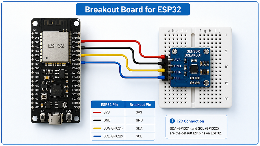
How to Connect a Breakout Board?
Connecting a breakout board depends on the component, interface, voltage level, and host controller. Still, most breakout boards follow a similar process.
1. Read the pin labels and datasheet
Before wiring, check the pin names, voltage range, interface type, and current requirements. Do not assume that all breakout boards use the same pin order.
2. Connect power and ground first
Most boards require VCC or VIN and GND. Confirm whether the board accepts 5 V, 3.3 V, or another voltage. ESP32-based systems usually operate at 3.3 V logic, even when some development boards accept 5 V through a regulator.
3. Connect the signal pins
For I2C, connect SDA and SCL.
For SPI, connect MOSI, MISO, SCK, and CS.
For UART, connect TX to RX and RX to TX.
For analog output, connect the signal pin to an ADC input.
For digital output, connect the pin to a GPIO.
4. Check logic voltage compatibility
A 5 V signal connected directly to a 3.3 V ESP32 GPIO may damage the chip. Use level shifting when needed.
5. Add pull-up resistors when required
Some breakout boards already include pull-up resistors. Others do not. I2C lines usually need pull-ups to the correct logic voltage.
6. Keep wiring short for sensitive signals
Long jumper wires may create noise, ringing, or communication errors. For high-speed signals, a custom PCB is better than loose wiring.
7. Test with simple code or basic measurements
Confirm power voltage, device address, communication response, and basic output before building a larger system.
For a breakout board for ESP32, always pay attention to 3.3 V logic, bootstrapping pins, current demand, antenna clearance, and GPIO functions. Some ESP32 pins have special behavior during startup, so pin selection matters.
Applications and Uses of Breakout Boards
Breakout boards are used across many fields, from hobby electronics to professional engineering.
- Embedded system development
- ESP32 and IoT projects
- PCB prototyping
- Production testing
- Repair and reverse engineering
- Education and training
- Industrial control prototypes
- Medical, automotive, and aerospace electronics evaluation
In high-reliability industries, breakout boards may be used for early validation, test planning, component qualification, and interface checking before formal product development.
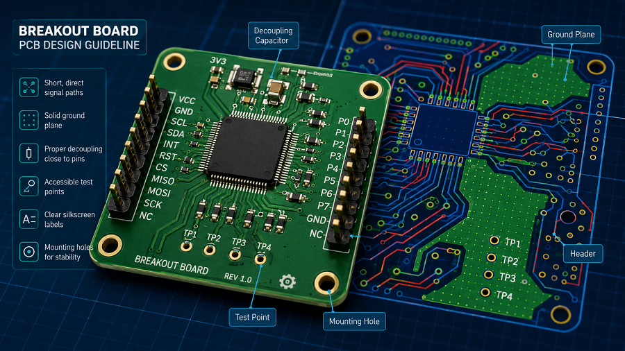
Breakout Board PCB Design Guideline
A good breakout board PCB design should not only expose pins. It should also protect signal quality, simplify assembly, and make debugging easier. Below are practical design guidelines.
1. Define the purpose before layout
Start by deciding what the board needs to do. Is it only an adapter? Does it need power regulation? Will it support breadboard use? Will it be mounted inside a test fixture? Will it be used by engineers, customers, or production operators?
The purpose affects size, connector choice, silkscreen labeling, mounting holes, and protection circuits.
2. Choose the right connector style
For breadboard use, 2.54 mm through-hole headers are common. For compact integration, castellated holes may be better. For field wiring, screw terminals or spring terminals are easier to handle. For test fixtures, pogo-pin pads may be preferred.
Connector selection should match how the board will actually be used.
3. Keep pinout logical
A good pinout reduces mistakes. Place power and ground pins clearly. Group communication pins together. For example, I2C pins should be near each other, and SPI pins should be organized in a readable sequence.
For ESP32 breakout boards, group GPIO pins by function when possible, such as ADC pins, UART pins, SPI pins, I2C pins, and power pins.
4. Use clear silkscreen
Silkscreen is not decoration. It is part of the user interface. Label every important pin. Mark voltage levels. Indicate pin 1. Add polarity marks for diodes, capacitors, power connectors, and LEDs.
Avoid placing text under components or too close to pads where solder may cover it.
5. Add decoupling capacitors close to power pins
Place decoupling capacitors near the power pins of the IC or module. Short traces help reduce power noise and improve circuit stability.
For many ICs, a 0.1 µF capacitor is placed close to each power pin, with additional bulk capacitance when needed.
6. Consider signal integrity
For low-speed GPIO or simple analog signals, routing is usually straightforward. For USB, high-speed SPI, RF, Ethernet, HDMI, or fast clocks, layout needs more care.
Controlled impedance, short trace length, solid ground reference, differential pair routing, and proper return paths may be required.
7. Use a solid ground plane when possible
Even on a small 2-layer breakout board, a solid ground plane improves stability, reduces noise, and gives signals a better return path.
Avoid cutting the ground plane unnecessarily. Keep high-current paths and sensitive analog signals separated when practical.
8. Protect exposed interfaces
Breakout boards are often handled, touched, rewired, and tested repeatedly. This increases the chance of ESD, reverse connection, or accidental short circuits.
Useful protection methods include:
- ESD protection diodes for external connectors
- Series resistors for signal protection
- Resettable fuse for power input
- Reverse polarity protection
- TVS diodes for power or communication lines
- Clear polarity marking on silkscreen
9. Include test points
Test points are valuable during debugging and manufacturing. At minimum, consider adding test points for power, ground, reset, communication lines, and important control signals.
For production use, test points can support ICT, flying probe testing, or functional test fixtures.
10. Review the design before fabrication
Before sending files to a PCB manufacturer, check:
- Schematic correctness
- Footprint accuracy
- Pin mapping
- Power polarity
- DRC errors
- Silkscreen readability
- Connector orientation
- Mounting hole position
- Board outline
- Gerber files
- BOM accuracy
- Assembly drawing
At EBest Circuit, breakout board PCB projects can be supported from PCB fabrication to assembly and testing. For customers developing sensor modules, ESP32-related hardware, connector adapters, or custom evaluation boards, early DFM review helps catch layout, soldering, and manufacturability issues before production.
FAQs
1. Do you need a breakout board?
You need a breakout board when a component is difficult to connect directly, especially if it uses fine-pitch pins, SMD packaging, dense connectors, or special voltage requirements. A breakout board is also useful when you want to test a component before designing it into a final PCB.
For simple through-hole components, you may not need one. For sensors, modules, USB connectors, ESP32 peripherals, and small IC packages, a breakout board can save time and reduce wiring errors.
2. What is a USB breakout board?
A USB breakout board is a small PCB that exposes the pins of a USB connector to larger pads or headers. It may be used for USB power testing, data line measurement, connector evaluation, repair work, or custom device development.
A USB breakout board may expose VBUS, GND, D+, D-, shield, CC pins, SBU pins, or SuperSpeed differential pairs, depending on whether it uses USB 2.0, USB 3.x, Micro USB, Mini USB, USB-A, or USB Type-C.
3. What is the difference between a breakout board and a development board?
A breakout board usually exposes the pins of one component, connector, sensor, or module. A development board is usually a more complete platform that includes a microcontroller or processor, power circuit, programming interface, reset circuit, clock source, connectors, and sometimes built-in debugging support.
4. How do you choose the right breakout board for ESP32 projects?
To choose the right breakout board for ESP32 projects, check the ESP32 module type, pinout, voltage input, available GPIO pins, USB interface, programming method, mounting style, and antenna clearance.
Also confirm whether the board supports your required functions, such as ADC, I2C, SPI, UART, PWM, battery power, sensor connection, relay control, or display interface. For stable wireless performance, avoid placing copper, metal parts, or tall components too close to the ESP32 antenna area.
5. Can I design a custom breakout board PCB for my own component?
Yes. You can design a custom breakout board PCB for almost any component, including sensors, ICs, connectors, power modules, wireless modules, and display interfaces.
A custom board is useful when standard breakout boards do not match your pinout, size, voltage, connector style, or testing method. For better results, start with the component datasheet, create an accurate schematic, verify the footprint, add proper power filtering, label the pins clearly, and review the Gerber files before fabrication.
Tags: breakout board, breakout board for esp32, breakout board pcb, breakout board pcb design, breakout board vs breadboard
PakarPBN
A Private Blog Network (PBN) is a collection of websites that are controlled by a single individual or organization and used primarily to build backlinks to a “money site” in order to influence its ranking in search engines such as Google. The core idea behind a PBN is based on the importance of backlinks in Google’s ranking algorithm. Since Google views backlinks as signals of authority and trust, some website owners attempt to artificially create these signals through a controlled network of sites.
In a typical PBN setup, the owner acquires expired or aged domains that already have existing authority, backlinks, and history. These domains are rebuilt with new content and hosted separately, often using different IP addresses, hosting providers, themes, and ownership details to make them appear unrelated. Within the content published on these sites, links are strategically placed that point to the main website the owner wants to rank higher. By doing this, the owner attempts to pass link equity (also known as “link juice”) from the PBN sites to the target website.
The purpose of a PBN is to give the impression that the target website is naturally earning links from multiple independent sources. If done effectively, this can temporarily improve keyword rankings, increase organic visibility, and drive more traffic from search results.
Comments are closed, but trackbacks and pingbacks are open.