A tunnel diode, also called an Esaki diode, is a heavily doped PN-junction diode that uses quantum tunneling to conduct current. Unlike a conventional diode, its forward current can decrease as voltage increases, creating a region of negative differential resistance. This characteristic makes tunnel diodes useful in certain high-frequency oscillators, amplifiers, and fast-switching circuits.
Understanding the relationship between quantum tunneling, I–V characteristics, and external circuit conditions explains why tunnel diodes behave differently from ordinary semiconductor diodes and how their properties can be used in practical electronic circuits.
What Is a Tunnel Diode?
A tunnel diode is a two-terminal semiconductor device with a heavily doped PN junction and an extremely narrow depletion region. Its defining feature is negative differential resistance, which occurs over a particular range of forward voltage.
The device is also known as an Esaki diode, named after physicist Leo Esaki, who discovered electron tunneling in heavily doped semiconductor junctions in 1957. Unlike ordinary rectifier diodes, tunnel diodes allow electrons to pass through the thin junction barrier by quantum tunneling at relatively low forward voltages.
A tunnel diode has an anode and a cathode, but its schematic symbol differs from that of an ordinary diode through a modified cathode marking. Since package markings and symbol conventions may vary, terminal identification should be confirmed using the manufacturer’s documentation.
How Does a Tunnel Diode Work?
A tunnel diode operates through quantum tunneling, a process that allows electrons to pass through an energy barrier they could not cross according to classical physics alone. Heavy doping narrows the PN-junction depletion region to only a few nanometers, making tunneling significant.
The high doping concentration also changes the semiconductor’s energy-band structure. In a typical Esaki diode, occupied electron states extend into the N-type conduction band, while available states exist in the P-type valence band. The alignment between these states determines how many electrons can tunnel across the junction.
At zero bias, electrons can tunnel in both directions, but the opposing currents balance under thermal equilibrium. Consequently, no net external current flows through the device.
When a small forward voltage is applied, the energy bands shift relative to each other. Occupied states on the N-side align with available states on the P-side, allowing electrons to tunnel through the barrier. As this alignment initially improves, the forward current increases.
Beyond a certain voltage, further increases in forward bias reduce the overlap between occupied and available energy states. The tunneling current then decreases even though the forward voltage continues to rise. This behavior produces the negative differential resistance region.
At higher forward voltages, conventional carrier injection becomes increasingly significant, and the total current begins rising again. These changes in conduction mechanisms explain the distinctive I–V characteristics of a tunnel diode.
What Does the Tunnel Diode I–V Curve Show?
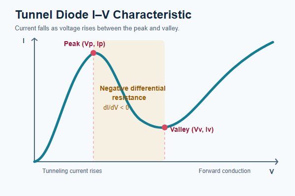
The tunnel diode I–V curve shows how current changes with applied voltage. Unlike the forward characteristic of a conventional diode, it contains a peak, a valley, and a region where current decreases as voltage increases.
Four parameters define the main points on the curve:
| Parameter | Description |
| Peak Voltage (Vp) | Voltage at the initial current peak |
| Peak Current (Ip) | Maximum initial tunneling current |
| Valley Voltage (Vv) | Voltage at the current valley |
| Valley Current (Iv) | Minimum current after the peak |
These points divide the forward characteristic into three operating regions.
Before the peak, forward current increases with voltage as the alignment of available tunneling states improves. The current reaches its initial maximum at the peak point, defined by Vp and Ip.
Between the peak and valley, increasing voltage reduces the available tunneling transitions. Current falls from Ip toward Iv, producing negative differential resistance, expressed as:
dIdV < 0
This means that a small increase in voltage causes a decrease in current. It does not mean the diode has negative static resistance. Under positive forward voltage and current, V/I remains positive, while the local differential resistance dV/dI is negative.
Beyond the valley, conventional forward conduction becomes dominant, and current increases again with voltage.
Another characteristic is the peak-to-valley current ratio (Ip/Iv), which indicates the current contrast between the two points. A higher ratio can benefit certain switching and bistable circuits, although it does not describe the entire negative-resistance region.
Differential resistance depends on the local slope of the I–V curve and changes with the operating point. Two tunnel diodes with similar peak-to-valley ratios may therefore respond differently under the same external circuit conditions.
How Do Bias and Load Conditions Affect a Tunnel Diode?
A tunnel diode’s operating behavior depends on its I–V characteristics and the external circuit. Bias voltage and load resistance determine the possible operating points, while capacitance, inductance, and circuit losses influence dynamic stability.
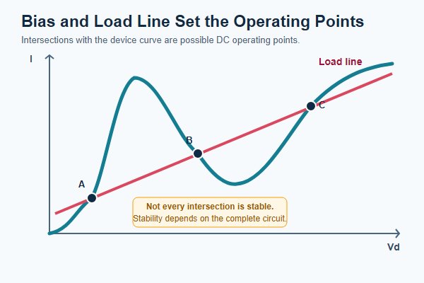
Consider a DC voltage source connected to a tunnel diode through a series resistor. The resistor establishes a load line that describes the relationship between diode voltage and current:
I = Vs − VdR
Here, Vs is the supply voltage, Vd is the diode voltage, and R is the series resistance. The intersections between this load line and the diode’s I–V curve represent possible DC operating points.
Because the tunnel diode characteristic rises, falls, and rises again, the load line may intersect it at several points. However, not every operating point is necessarily stable.
For example, consider a 0.50 V supply and a 500 Ω series resistor. At a diode voltage of 65 mV, the load-line current is:
I = (0.50 − 0.065) / 500 = 0.87 mA
At 350 mV, the same circuit produces a load-line current of 0.30 mA.
These voltages correspond to published typical peak and valley voltages for the 1N3712 tunnel diode. Comparing the load-line values with the device’s nominal peak current of 1.0 mA and maximum valley current of 0.18 mA illustrates how multiple intersections can occur.
This is an illustrative calculation, not a verified measurement of one physical device. Exact operating points and their stability must be determined from the actual I–V characteristic and the complete circuit.
Under suitable conditions, multiple stable operating points can produce bistable switching behavior. When a resonant network is added, the diode’s negative differential resistance may also support oscillation.
How Does a Tunnel Diode Oscillator Work?
A tunnel diode oscillator uses negative differential resistance to sustain oscillations in an LC resonant circuit. When the diode is biased within its negative-resistance region, it can compensate for energy lost in the resonant network. Oscillation begins when the circuit satisfies the required startup conditions.
The circuit typically includes a tunnel diode, a DC bias network, and an LC resonant network. The bias network establishes the diode’s operating point, while the inductor and capacitor determine the approximate resonant frequency. For an ideal LC circuit, the frequency is:
f = 12π√(LC)
Here, L represents inductance in henries (H), and C represents capacitance in farads (F). In a practical oscillator, junction capacitance, package parasitics, and PCB interconnections can change the effective resonant values and shift the actual oscillation frequency.
Real LC circuits lose energy through resistance and external loading. In a parallel resonant model, oscillation can start when the magnitude of the diode’s negative differential conductance exceeds the total positive loss conductance. Small electrical disturbances then grow into oscillations.
As the amplitude increases, the diode’s nonlinear I–V characteristic limits further growth until the energy supplied balances circuit losses. The operating conditions required for startup therefore differ from those governing the final oscillation amplitude.
Proper biasing and low-loss connections are essential for reliable operation. Excessive circuit losses or an unsuitable operating point may prevent oscillation. At high frequencies, short connections, controlled return-current paths, and appropriate bias decoupling help reduce unwanted parasitic effects on the PCB.
What Are Tunnel Diodes Used For?
Tunnel diodes have been used in specialized circuits that benefit from fast tunneling response and negative differential resistance. Although modern transistors and integrated circuits have replaced many traditional applications, tunnel diodes remain relevant to certain nonlinear and high-frequency circuits.
Their main applications include:
- High-frequency amplification: A tunnel diode operating in its negative differential resistance region can provide small-signal gain. Circuit impedance, loading, and stability determine the usable frequency range.
- Pulse generation: The nonlinear I–V characteristic supports rapid transitions between operating states. Tunnel diode pulse circuits have historically been used in high-speed measurement and triggering equipment.
- High-speed switching: Suitable bias and load conditions allow a circuit to switch between operating states. Switching behavior depends on the external circuit and parasitic elements.
- Bistable circuits: Certain load-line conditions produce two stable operating states. An input signal can move the circuit between them, supporting specialized switching and memory functions.
- RF and microwave circuits: Negative differential resistance can support specialized oscillators and amplifiers. Junction capacitance, package inductance, and impedance matching become particularly significant at high frequencies.
Each application uses the same nonlinear characteristic in a different way. A tunnel diode should therefore be selected according to the required circuit function, operating conditions, and performance limits rather than tunneling speed alone.
What Are the Advantages and Limitations of Tunnel Diodes?
Tunnel diodes offer fast electrical response, negative differential resistance, and useful nonlinear behavior at relatively low forward voltages. These characteristics make them suitable for specialized circuits, although their performance and availability impose practical restrictions.
Their main advantages include:
- Fast response: Quantum tunneling does not depend on conventional minority-carrier storage during forward conduction.
- Negative differential resistance: Supports specialized oscillation, amplification, and switching functions.
- Low-voltage operation: Certain circuits can operate within the tunneling region at relatively small forward voltages.
- Simple device structure: A two-terminal junction provides nonlinear electrical behavior without a conventional multi-terminal active device.
However, tunnel diodes also have limitations:
- Limited output power: Conventional tunnel diodes generally have restricted power capability.
- Bias sensitivity: Voltage and load changes may move the operating point outside the intended region.
- Parasitic effects: Junction capacitance, series resistance, and package inductance affect high-frequency performance.
- Component availability: Some traditional models are obsolete or available only through specialized suppliers.
Modern transistors and integrated circuits are often more practical for common oscillator and switching applications. Tunnel diodes are most suitable when their negative differential resistance provides a specific advantage that justifies these constraints.
Which Tunnel Diode Specifications Matter Most?
Tunnel diode selection begins with the required circuit behavior. Peak and valley characteristics define the nonlinear operating region, while capacitance, resistance, and maximum ratings influence practical performance.
The 1N3712 germanium tunnel diode provides a useful reference. Published supplier specifications include the following values:
| Parameter | 1N3712 Value | Specification Type |
| Peak Current (Ip) | 1.0 mA | Nominal |
| Peak Voltage (Vp) | 65 mV | Typical |
| Valley Current (Iv) | 0.18 mA | Maximum |
| Valley Voltage (Vv) | 350 mV | Typical |
| Junction Capacitance | 10 pF | Maximum |
| Series Resistance | 4 Ω | Maximum |
These figures illustrate why a tunnel diode cannot be selected using a single current or voltage rating. The peak and valley characteristics identify the approximate negative-resistance region, while capacitance and resistance influence high-frequency behavior.
For an oscillator, the differential resistance at the selected bias point must provide sufficient negative conductance to overcome circuit losses. For switching applications, the peak-to-valley characteristics and load-line intersections help determine the available operating states.
The peak-to-valley current ratio, temperature behavior, maximum electrical ratings, and device package should also be reviewed. Two devices with similar peak currents may behave differently because of variations in their valley characteristics, capacitance, or differential resistance.
A suitable tunnel diode must be evaluated using its complete I–V characteristics and operating limits. Similar package dimensions or nominal peak-current ratings alone do not guarantee equivalent circuit performance.
Common Questions About Tunnel Diodes
Q1: Can You Test a Tunnel Diode with a Multimeter?
A1: A multimeter can provide a basic conduction check, but it cannot reliably verify the negative differential resistance region. A controlled, current-limited I–V measurement is more suitable for evaluating a tunnel diode’s characteristics.
Q2: Can a Tunnel Diode Be Simulated in SPICE?
A2: Yes. A tunnel diode can be simulated using a nonlinear SPICE model that reproduces its negative differential resistance. Oscillator simulations should also account for junction capacitance, parasitic resistance, inductance, and bias conditions.
Q3: What Happens When a Tunnel Diode Is Reverse-Biased?
A3: A tunnel diode can conduct substantial reverse current through quantum tunneling, even at relatively low voltages. Current limiting is essential because excessive reverse current or power dissipation can damage the device.
Q4: Can a Tunnel Diode Operate at Zero Bias?
A4: Quantum tunneling can occur at zero bias, but opposing electron flows balance under thermal equilibrium, producing no net external current. Applying a voltage changes the energy-band alignment and creates a net current.
Q5: Does Temperature Affect Tunnel Diode Performance?
A5: Yes. Temperature can change peak and valley currents, affecting bias stability and circuit performance. Temperature-dependent I–V characteristics should be considered when selecting a tunnel diode for a wide operating temperature range.
Q6: Is a Backward Diode the Same as a Tunnel Diode?
A6: Not exactly. A backward diode is a related tunneling device designed for useful conduction at low reverse voltages. Unlike a conventional Esaki tunnel diode, it typically has a reduced forward tunneling peak and is often used for low-level signal detection.
Q7: How Is an Esaki Diode Different from a Resonant Tunneling Diode?
A7: An Esaki diode uses band-to-band tunneling through a heavily doped PN junction. A resonant tunneling diode (RTD) uses engineered quantum structures, typically involving a quantum well and tunneling barriers. Their operating mechanisms and applications differ.
Q8: Can Excessive Current Damage a Tunnel Diode?
A8: Yes. Excessive current, voltage, or power dissipation can damage the semiconductor junction. Check the device’s maximum ratings and use suitable current limiting, particularly when testing older or difficult-to-replace components.
Q9: Are Tunnel Diodes Still Available for New Designs?
A9: Yes, some tunnel diodes remain available from specialized suppliers, although many older models are obsolete. Verify stock, device specifications, and long-term availability before selecting one for a new production design.
Q10: Can an Obsolete Tunnel Diode Be Replaced with Another Model?
A10: Possibly, but matching the package or peak current alone is insufficient. Compare peak and valley characteristics, differential resistance, junction capacitance, and operating limits before evaluating a replacement in the original circuit.
Conclusion
A tunnel diode uses quantum tunneling to produce negative differential resistance, enabling specialized functions in oscillators, amplifiers, and switching circuits. Its I–V characteristics, bias conditions, and device specifications must be considered together when evaluating circuit performance.
For projects involving specialized semiconductor devices, EBest Circuit provides PCB manufacturing, PCBA assembly, and manufacturing-related technical guidance. Contact sales@bestpcbs.com to discuss your PCB specifications, BOM, production requirements, or quotation.
This entry was posted on Friday, October 9th, 2026 at 6:05 pm and is filed under Electronic Components.
You can follow any responses to this entry through the RSS 2.0 feed.
You can skip to the end and leave a response. Pinging is currently not allowed.
PakarPBN
A Private Blog Network (PBN) is a collection of websites that are controlled by a single individual or organization and used primarily to build backlinks to a “money site” in order to influence its ranking in search engines such as Google. The core idea behind a PBN is based on the importance of backlinks in Google’s ranking algorithm. Since Google views backlinks as signals of authority and trust, some website owners attempt to artificially create these signals through a controlled network of sites.
In a typical PBN setup, the owner acquires expired or aged domains that already have existing authority, backlinks, and history. These domains are rebuilt with new content and hosted separately, often using different IP addresses, hosting providers, themes, and ownership details to make them appear unrelated. Within the content published on these sites, links are strategically placed that point to the main website the owner wants to rank higher. By doing this, the owner attempts to pass link equity (also known as “link juice”) from the PBN sites to the target website.
The purpose of a PBN is to give the impression that the target website is naturally earning links from multiple independent sources. If done effectively, this can temporarily improve keyword rankings, increase organic visibility, and drive more traffic from search results.
Comments are closed, but trackbacks and pingbacks are open.