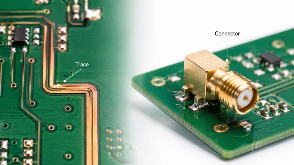
A right angle PCB usually has two meanings: one refers to a PCB trace that turns at a 90-degree angle, and the other refers to a right angle PCB connector, header, or mount component installed horizontally on the board. In PCB layout, 90-degree traces can be acceptable for simple low-speed circuits, but they are not the best choice for high-speed, RF, clock, or impedance-controlled signals. For safer routing and better design margin, 45-degree, curved, or mitered traces are usually preferred.
If your project involves right angle PCB traces, right angle PCB connectors, RF connectors, or compact mechanical design, Best Technology can provide one-stop support from PCB fabrication to PCBA assembly, including FR4 PCB, high-speed PCB, RF PCB, impedance control PCB, connector assembly, and full board testing. Our engineering team can review Gerber files, BOM, connector footprints, PCB Routing Angle Rules, DFM risks, and assembly feasibility before production to help reduce rework risks in both prototyping and mass production. Send your Gerber files, BOM, connector datasheets, and quantity requirements to sales@bestpcbs.com for engineering review and quotation.
What Does Right Angle PCB Mean?
A right angle PCB usually refers to either a PCB trace with a 90-degree turn or a PCB-mounted component installed at a 90-degree orientation.
Right Angle PCB Trace
A right angle PCB trace is a copper trace that changes direction sharply at 90 degrees. Instead of using two 45-degree bends or a smooth curve, the route turns with a square corner.
This matters because a PCB trace carries current, forms an electromagnetic field, and depends on a clean return path. When the trace shape changes suddenly, its electrical behavior may also change.
Right Angle PCB Connector or Mount
A right angle PCB connector is mounted so the mating direction runs parallel to the PCB surface. It is often used when the product needs a side-entry cable, edge connection, compact enclosure, or horizontal board-to-board connection.
Common examples include:
- Right angle PCB connector
- Right angle PCB header
- Right angle SMA connector
- Right angle BNC connector
- Right angle PCB terminal
- Right angle switch
- Right angle potentiometer
Why This Difference Matters
A right angle connector can be a good mechanical choice. A right angle trace may be a layout concern. The connector itself can be designed for 90-degree mounting, but the trace connected to it still needs proper routing, grounding, solder pad design, and manufacturability review.
| Term | Meaning | Main Concern |
|---|---|---|
| Right angle trace | 90-degree copper route | Signal, EMI, impedance |
| Right angle connector | Side-entry connector | Footprint, soldering |
| Right angle mount | 90-degree component | Clearance, strength |
| Right angle header | Horizontal pin header | Alignment, mating |
For a real PCB project, both layout and assembly details should be checked before production.
Are 90-Degree PCB Traces Bad?
90-degree PCB traces are not automatically bad, but they should be avoided on critical signals. They are usually acceptable in low-speed circuits, but not ideal for high-speed, RF, clock, or controlled-impedance routing.
The old rule “never use right angle traces” is too simple. The real answer depends on the signal type, frequency, edge rate, trace length, stack-up, and manufacturing tolerance.
Right Angle Traces Are Usually Acceptable When:
- The signal is low speed.
- The trace is short.
- The board has no strict impedance requirement.
- The design is not RF or microwave.
- The circuit is simple control, relay, LED, or low-frequency.
- The manufacturer’s design rules allow it.
In these cases, a right angle trace may not cause any measurable issue.
Right Angle Traces Should Be Avoided When:
- The trace carries USB, HDMI, PCIe, Ethernet, LVDS, DDR, or MIPI signals.
- The route is part of a clock circuit.
- The trace requires controlled impedance.
- The circuit includes RF or antenna signals.
- The trace is near an SMA or BNC connector launch.
- The product has strict EMI or reliability requirements.
For these applications, a smoother route is safer.
Manufacturing Tip: A PCB manufacturer can usually fabricate right angle traces. The better question is whether that geometry is suitable for the signal, stack-up, copper thickness, and final application.
Why Do PCB Designers Avoid Right Angle Traces?
Designers avoid right angle traces because sharp corners can create small impedance discontinuities, increase EMI risk, affect signal quality, and reduce layout margin in sensitive circuits.
A single 90-degree corner may not destroy a board. But good PCB design is about reducing avoidable risks before production.
1. Impedance Discontinuity
- Controlled impedance depends on trace width, copper thickness, dielectric thickness, dielectric constant, solder mask, and distance to the reference plane. At a right angle corner, the copper area becomes slightly larger than the straight trace section.
- This extra copper area can behave like a small capacitive discontinuity. In low-speed circuits, it may not matter. In high-speed or RF circuits, it can affect signal behavior.
2. Signal Reflection
Fast digital signals can behave like transmission-line signals. When they meet a sudden geometry change, part of the signal energy may reflect back.
Possible results include:
- Ringing
- Overshoot
- Undershoot
- Timing uncertainty
- Lower signal margin
This is more important in high-speed buses, clock lines, and impedance-controlled differential pairs.
3. EMI Risk
- A sharp trace corner can disturb the field around the trace. If the return path is also poor, the loop area may increase. A larger loop area can increase radiated noise.
- The corner itself is usually not the only EMI cause. Poor grounding, bad return paths, long loops, and connector transitions often matter more. Still, avoiding sharp corners is part of good layout practice.
4. Fabrication Margin
- In older PCB manufacturing, sharp inner corners could create acid trap concerns during etching. Modern PCB fabrication has improved, so this issue is less severe today.
- However, smoother routing still gives cleaner copper definition and a more professional layout. It also reduces unnecessary questions during DFM review.
Engineering Tip: Do not focus only on the corner. A good PCB manufacturer will also check trace width, spacing, copper balance, via placement, reference plane continuity, and connector footprint accuracy.
When Are Right Angle PCB Traces Acceptable?
Right angle PCB traces are acceptable when the circuit is low speed, the trace is short, the signal is not impedance controlled, and the layout does not involve RF or strict EMI requirements.
A practical design should not treat every 90-degree corner as a failure. Some boards are simple. Some traces are not sensitive. Some design constraints also leave very little routing space.
Acceptable Use Cases
Right angle traces may be acceptable in:
- LED control boards
- Relay control circuits
- Low-speed sensor boards
- Simple power control lines
- Short GPIO routes
- Basic industrial control signals
- Non-critical test points
- Low-frequency analog sections
In these cases, the performance impact is often very small.
Use More Caution In These Cases
Right angle traces should be reviewed carefully when the design includes:
- High-speed digital interfaces
- RF circuits
- Antenna feeds
- Clock traces
- Differential pairs
- Impedance-controlled routing
- Long traces near the board edge
- Medical, automotive, aerospace, or industrial reliability needs
These products usually need more predictable routing and stronger design control.
Simple Decision Table
| Situation | Right Angle? | Better Choice |
|---|---|---|
| Low-speed short trace | Usually OK | 45-degree |
| LED / relay control | Usually OK | 45-degree |
| High-speed trace | Avoid | 45-degree |
| RF / antenna trace | Avoid | Curved |
| Impedance line | Avoid | Smooth route |
| Power trace | Depends | Wide copper |
Manufacturing Tip: Before production, the real question is not only “Is this right angle trace allowed?” The better question is: Will this routing affect signal performance, manufacturing quality, or long-term reliability?
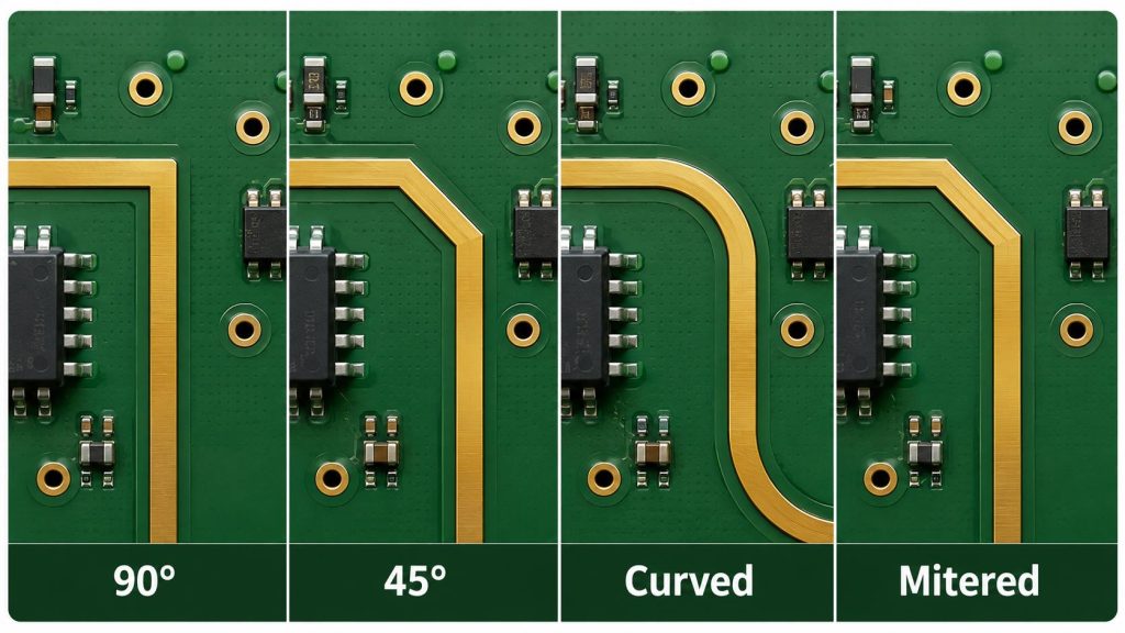
Right Angle vs 45-Degree vs Curved PCB Traces
For most PCB layouts, two 45-degree bends are better than one 90-degree bend. For RF and high-frequency designs, curved or mitered traces are often preferred.
The best routing style depends on the circuit type.
| Trace Style | Best For | Note |
|---|---|---|
| 90-degree | Low-speed routing | Use only when needed |
| 45-degree | General PCB layout | Best default choice |
| Curved | RF / antenna | Smoothest transition |
| Mitered | High frequency | Needs design control |
Why 45-Degree Routing Is Common
Two 45-degree bends reduce sudden geometry change. They are easy to route, easy to manufacture, and widely accepted as a clean PCB layout practice.
This is why many CAD tools use 45-degree routing as the standard setting.
When Curved Routing Makes Sense
Curved routing is useful for:
- RF traces
- Antenna feed lines
- Microwave circuits
- Precision analog routes
- High-frequency connector launch areas
Curved routes provide a smoother field transition and can help maintain more stable impedance behavior.
When Mitered Corners Are Useful
Mitered corners are often used in high-frequency layouts. A miter cuts away part of the right angle corner to reduce excess capacitance.
This can be useful, but it should not be applied randomly. The layout should match the impedance requirement, stack-up, frequency range, and design guidance.
Practical Recommendation: Use 45-degree bends as the default. Use curved or mitered traces for RF and high-frequency areas. Avoid 90-degree routing on sensitive signals unless there is a clear reason.
Where Do Right Angle Traces Matter Most?
Right angle traces matter most in high-speed, RF, clock, impedance-controlled, and EMI-sensitive PCB designs.
In these applications, the copper trace behaves more like a controlled transmission path. Small geometry changes can become more important.
High-Speed Digital Circuits
High-speed interfaces need consistent routing. These may include:
- USB
- HDMI
- PCIe
- Ethernet
- MIPI
- LVDS
- DDR memory interfaces
For these signals, trace impedance, pair spacing, length matching, via transitions, and reference plane continuity all matter. A right angle bend may not be the biggest issue, but it adds one more discontinuity.
RF and Antenna Circuits
RF PCB design is more sensitive to geometry. Around an SMA connector right angle PCB area or a BNC connector PCB mount right angle area, the connector launch and nearby trace routing should be carefully controlled.
Important RF checks include:
- Controlled impedance trace width
- Ground via placement
- Smooth connector-to-trace transition
- Short RF path
- Continuous ground reference
- Proper copper clearance
A right angle connector may be mechanically correct. But the RF trace leaving the connector should still be designed with controlled geometry.
Clock Lines
Clock signals affect the timing of the whole circuit. Poor clock routing can increase noise, jitter, and EMI.
For clock traces, designers should:
- Keep the path short.
- Avoid unnecessary corners.
- Maintain a continuous return path.
- Keep the trace away from noisy power circuits.
- Avoid routing near board edges when possible.
Power Circuits
Power traces are different from high-speed signal traces. Their main concerns are current capacity, voltage drop, copper thickness, heat spreading, and thermal reliability.
For power PCB design, use:
- Adequate trace width
- Proper copper thickness
- Smooth copper pours
- Strong via arrays
- Correct thermal relief design
- Enough electrical clearance
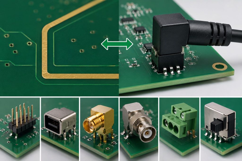
Right Angle PCB Connector vs Right Angle Trace
A right angle PCB connector is a mechanical component choice. A right angle trace is a copper routing shape. They should not be treated as the same design issue.
This distinction matters because many buyers search “right angle PCB” when they actually need connector assembly or PCB-mounted components.
Right Angle PCB Connector
A right angle PCB connector exits from the side of the board. It is commonly used when the product needs compact cable routing, edge connection, or enclosure compatibility.
Common applications include:
- Industrial controllers
- Communication modules
- Power supplies
- Automotive electronics
- Medical devices
- Consumer electronics
- Smart home products
Common Right Angle PCB-Mounted Parts
| Component | Typical Use |
|---|---|
| Right angle header | Board connection |
| Right angle connector | Cable connection |
| Right angle SMA | RF signal |
| Right angle BNC | RF / test |
| Right angle terminal | Power / signal |
| Right angle switch | User control |
| Right angle bracket | Support |
Assembly Risks to Check
Right angle connectors often need stronger process control than simple SMD parts.
Key risks include:
- Incorrect footprint
- Poor hole size
- Connector tilt
- Weak solder joints
- Enclosure misalignment
- Insufficient support
- Wrong orientation
- Clearance conflict
Manufacturing Tip: If your project includes right angle PCB connectors, send the connector datasheet and part number with your Gerber and BOM files. This helps the manufacturer check footprint accuracy, assembly direction, soldering process, and mechanical clearance.
Who Needs Right Angle PCB Manufacturing Support?
You may need right angle PCB manufacturing support if your design includes 90-degree traces, right angle connectors, RF connector launches, controlled impedance, or compact mechanical assembly requirements.
Not every PCB project needs deep engineering review. But some boards benefit from manufacturer input before production.
You Should Contact a PCB Manufacturer If You Are:
- Unsure whether right angle traces need to be changed
- Designing a high-speed or RF PCB
- Using SMA, BNC, or other RF connectors
- Using right angle PCB headers or terminals
- Building a compact product with tight enclosure space
- Requiring controlled impedance
- Moving from prototype to mass production
- Experiencing EMI, signal, or assembly issues
- Looking for PCB fabrication and assembly from one supplier
Industries That Often Need This Support
Right angle PCB design and connector assembly may appear in:
- Industrial control equipment
- Communication devices
- RF modules
- Medical electronics
- Automotive electronics
- LED control systems
- Power supplies
- Consumer electronics
- Smart home devices
- Test equipment
How Best Technology Can Help
Best Technology supports custom PCB and PCBA projects from prototype to production. For designs involving right angle traces or right angle PCB-mounted components, our engineering team can help review:
- Gerber files
- PCB stack-up
- Controlled impedance needs
- Right angle trace locations
- RF connector areas
- Connector footprints
- BOM part numbers
- Assembly direction
- DFM and DFA risks
- Testing requirements
This helps reduce avoidable production problems before fabrication starts.
What Can a PCB Manufacturer Check Before Production?
A PCB manufacturer can check whether your right angle traces, connector footprints, stack-up, impedance requirements, and assembly details are suitable for reliable production.
Knowing the design rule is helpful. Confirming your actual file is better.
Design Checks Before Fabrication
A manufacturer can review:
- Trace width and spacing
- Right angle trace locations
- High-speed routing
- Differential pair spacing
- Controlled impedance
- Reference plane continuity
- Via placement
- Copper balance
- Solder mask clearance
- Board edge clearance
- Drill size
- Surface finish
Connector and Assembly Checks
For right angle PCB connectors and mounts, the review should include:
- Connector footprint
- Hole size
- Pad size
- Pin pitch
- Connector orientation
- Mechanical clearance
- Enclosure alignment
- Solder joint access
- Soldering method
- Inspection access
RF and High-Speed Checks
If the PCB includes RF or high-speed signals, the manufacturer may also check:
- Impedance stack-up
- RF trace width
- Ground via stitching
- Connector launch
- Return path
- Layer transition
- Board edge distance
- Nearby noise sources
What Files Should You Send for a Quote?
To get a faster and more accurate quotation, send:
- Gerber files
- Drill file
- BOM file
- Pick-and-place file
- PCB stack-up
- Board thickness
- Copper thickness
- Surface finish
- Solder mask color
- Quantity
- Connector datasheets
- Testing requirements
- Packaging needs
If your design includes right angle PCB traces, right angle PCB connectors, SMA/BNC connectors, or impedance-controlled routing, you can send your files to Best Technology for engineering review and quotation. A short review before production can help prevent layout, assembly, and reliability problems later.
FAQs About Right Angle PCB
Q1: Are right angle PCB traces always wrong?
No. Right angle PCB traces can work in many low-speed and non-critical circuits. However, they are usually avoided in high-speed, RF, clock, and impedance-controlled designs.
Q2: Why do PCB designers prefer 45-degree traces?
45-degree traces create a smoother copper transition than 90-degree traces. They are easy to route, easy to fabricate, and better for professional PCB layout quality.
Q3: Can right angle traces cause EMI?
They can contribute to EMI in sensitive circuits, especially when the return path is poor or the trace carries fast edges. However, EMI usually comes from several layout factors, not just one corner.
Q4: Do right angle traces matter in low-speed circuits?
Usually not much. In simple LED, relay, GPIO, and low-frequency control circuits, the practical effect is often very small.
Q5: Should RF PCB traces use curved routing?
Curved or mitered routing is often preferred for RF traces because it helps maintain smoother impedance behavior and avoids abrupt field changes.
Q6: What is a right angle PCB connector?
A right angle PCB connector is a connector mounted so the mating direction runs parallel to the board. It is common in compact devices, edge connections, and cable-to-board applications.
Q7: Is a right angle PCB connector the same as a right angle PCB trace?
No. A connector is a component and assembly issue. A trace is a copper routing issue. The connector may be right angle, but the trace connected to it should still follow good routing practice.
Q8: Can a PCB manufacturer fabricate right angle traces?
Yes. Modern PCB manufacturers can fabricate right angle traces. The more important question is whether those traces are suitable for your circuit and application.
Q9: What should I send for a right angle PCB quote?
You should send Gerber files, BOM, pick-and-place file, stack-up requirements, copper thickness, board thickness, quantity, connector part numbers, and any controlled impedance or testing requirements.
Q10: Can Best Technology review my right angle PCB design before production?
Yes. Best Technology can review Gerber files, connector footprints, impedance requirements, DFM risks, and assembly details before PCB fabrication and PCBA production.
In conclusion, a right angle PCB is not a simple “good or bad” topic. A 90-degree trace may be acceptable in low-speed circuits, but it is usually not the best choice for high-speed, RF, clock, or controlled-impedance routing. In most PCB layouts, two 45-degree bends are a cleaner and safer default. For RF and high-frequency circuits, curved or mitered routing may offer better performance.
Right angle PCB connectors are a different issue. They are useful for compact products, side-entry cables, edge connections, and enclosure-based electronics. But they require careful footprint checking, soldering control, mechanical clearance review, and assembly planning.
If your project includes right angle PCB traces, right angle PCB connectors, RF connectors, or tight mechanical requirements, Best Technology can support your project from engineering review to PCB fabrication and PCBA assembly. We can also review PCB Routing Angle Rules, including 45-degree and 90-degree routing angles, connector footprints, impedance requirements, and assembly risks before production. Send your Gerber files, BOM, connector datasheets, and quantity requirements to sales@bestpcbs.com for a practical review and quotation.
Tags: PCB right angle traces, right angle PCB, right angle PCB traces
PakarPBN
A Private Blog Network (PBN) is a collection of websites that are controlled by a single individual or organization and used primarily to build backlinks to a “money site” in order to influence its ranking in search engines such as Google. The core idea behind a PBN is based on the importance of backlinks in Google’s ranking algorithm. Since Google views backlinks as signals of authority and trust, some website owners attempt to artificially create these signals through a controlled network of sites.
In a typical PBN setup, the owner acquires expired or aged domains that already have existing authority, backlinks, and history. These domains are rebuilt with new content and hosted separately, often using different IP addresses, hosting providers, themes, and ownership details to make them appear unrelated. Within the content published on these sites, links are strategically placed that point to the main website the owner wants to rank higher. By doing this, the owner attempts to pass link equity (also known as “link juice”) from the PBN sites to the target website.
The purpose of a PBN is to give the impression that the target website is naturally earning links from multiple independent sources. If done effectively, this can temporarily improve keyword rankings, increase organic visibility, and drive more traffic from search results.
Comments are closed, but trackbacks and pingbacks are open.