Embedded PCB Antennas are antenna structures that are integrated directly into the copper layer of a printed circuit board, enabling wireless communications without the need for external antenna components. This article explains how embedded PCB antennas work, their design principles, general structures such as 2.4 GHz embedded PCB antenna designs, and how manufacturers optimize antenna performance for wireless products.
Wireless connectivity has become fundamental in modern electronics. From IoT sensors and smart home devices to wearable technology and industrial control systems, engineers are increasingly choosing antenna solutions that reduce product size, simplify assembly and lower costs. Embedded antennas fulfill this purpose by integrating RF functionality directly into the PCB itself. EBest Circuits specializes in RF antenna PCB design, prototyping and complete PCBA assembly. With over 20 years of experience in RF PCB manufacturing, we help engineers bring wireless products to market faster and more reliably. For questions or factory visits, please contact us at sales@bestpcbs.com.
Why are Embedded PCB Antennas Popular in Modern Electronics?
Electronic devices are becoming smaller and require more connectivity options. This trend makes traditional external antennas less practical in many applications.
Embedded antennas provide several advantages.
Space Saving Design
Embedded antenna PCB eliminates the need for external antennas or connectors. This is especially useful in compact products such as smart sensors, wearable devices, and IoT modules.
Lower Production Costs
Because the antenna is etched directly onto the copper layer of the PCB, no additional antenna components, coaxial connectors, or cables are required.
Improved Mechanical Reliability
The external antenna may break, become loose, or have a worn connector. The embedded PCB antenna eliminates this potential point of failure.
Simplified Product Design
Industrial designers often prefer products without visible antennas. Embedded antennas enable sleek product designs without sacrificing wireless functionality.
Due to these benefits, embedded antenna technology is widely used in modern electronic devices.
What is an Embedded PCB Antenna?
An embedded PCB antenna is an antenna structure made using copper traces on the PCB. Instead of installing separate antenna modules, engineers designed a special copper pattern that transmits RF signals.
These antennas operate using electromagnetic radiation produced by alternating current flowing through copper traces.
Typical characteristics include:
- Traces of copper act as radiating elements
- Integration into PCB layers or surface traces
- Connection to RF transceiver via 50 ohm impedance line
- Use of tuning components for impedance matching
Embedded antennas are typically used at frequencies such as:
| Frequency | Typical Application |
|---|---|
| 433MHz | Remote control |
| 868/915MHz | LoRa Communications |
| 2.4GHz | Wi-Fi/Bluetooth |
| 5GHz | High speed Wi-Fi |
| 13.56MHz | NFC system |
Among them, 2.4 GHz embedded PCB antenna is the most widely used due to the popularity of WiFi and Bluetooth devices.
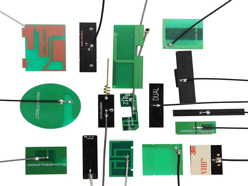
Embedded PCB Antenna Type
Different antenna structures are used depending on the frequency, PCB size, and product design constraints.
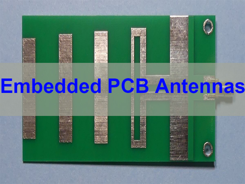
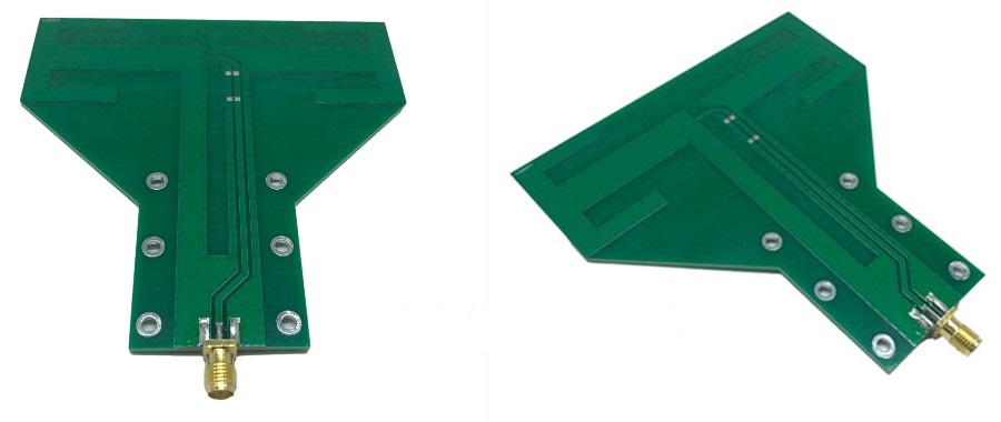
Inverted F Antenna (IFA)
The inverted F antenna is one of the most common PCB embedded antenna designs.
Its main characteristics include:
- Compact layout
- Good impedance matching
- Suitable for 2.4 GHz communications
This antenna structure is widely used in:
- WiFi Module
- Bluetooth device
- IoT communication module
PCB antenna winding
Winding antennas use winding copper traces that increase electrical length without increasing physical size.
The advantages include:
- Compact footprint
- Efficient low frequency operation
- Suitable for small devices
It is commonly used in:
- IoT Sensors
- LoRa devices
- wireless control module
Circle Antenna
A loop antenna consists of a closed copper loop that emits electromagnetic energy.
Common uses include:
- RFID system
- wireless communication device
- NFC system
In many smartphones and access control systems, the embedded nfc PCB antenna is implemented as a loop antenna around the PCB.
Patch Antenna
A patch antenna is a flat metal patch that is placed on a ground plane.
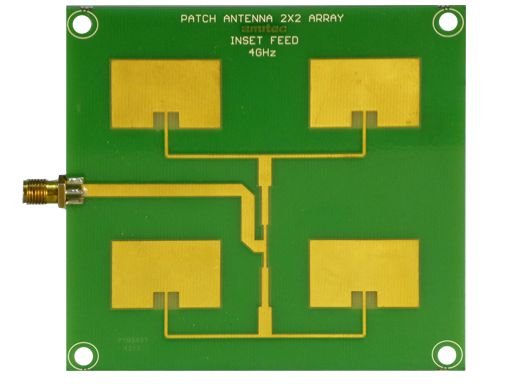
They provide:
- directed radiation
- higher profits
- stable performance
Applications include:
- GPS receiver
- satellite communications system
- automotive radar
How Does an Embedded PCB Antenna Work?
The embedded antenna converts electrical signals into electromagnetic waves. When RF current flows through the antenna trace, it produces an oscillating electromagnetic field that radiates out into space.
Radiation efficiency depends on several design factors.
Antenna Length
The main rule in antenna design is the quarter wavelength principle.
The approximate antenna length is:
| Frequency | Quarter Wavelength |
|---|---|
| 433MHz | ~17cm |
| 915MHz | ~8 cm |
| 2.4GHz | ~3.1cm |
Because space on a PCB is limited, engineers often use a sinuous structure to compress the length of the antenna.
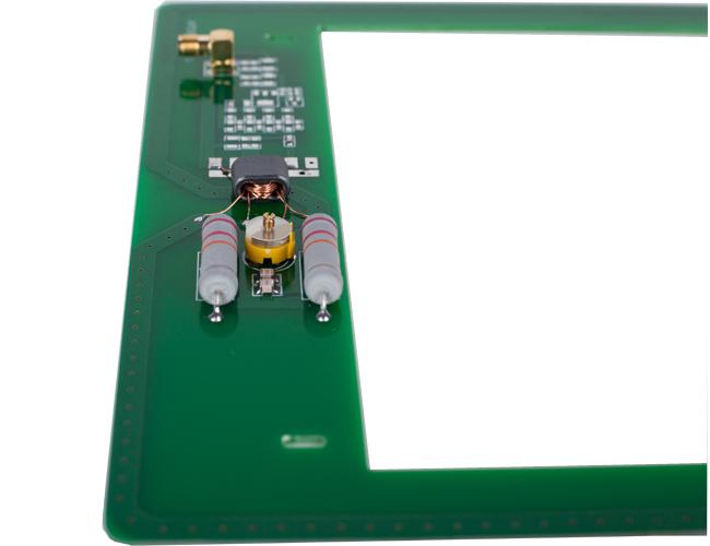
Impedance Matching
Most RF systems use an impedance of 50 ohms. If the antenna impedance does not match the RF circuit, signal reflection occurs.
Matching networks are commonly used.
Typical structures include:
- Pi matching network
- T matching network
- LC matching circuit
These components help optimize antenna efficiency and radiation performance.
Influence of Land Fields
The ground plane greatly influences antenna performance.
Key considerations include:
- Sufficient ground clearance around the antenna
- avoid large metal components nearby
- controlling the return flow path
Improper ground design can significantly reduce antenna efficiency.
Embedded PCB Antenna vs External Antenna
Engineers often choose between embedded antennas and external antennas depending on product requirements.
| Feature | Embedded PCB antenna | External Antenna |
|---|---|---|
| Size | Very compact | Bigger |
| Cost | Lower | Higher |
| RF performance | Currently | Usually stronger |
| Integration | Tall | Low |
| Mechanical reliability | Tall | Depends on the connector |
External antennas are often preferred when:
- maximum transmission distance required
- RF performance is very important
- The PCB size is very small
Embedded antennas are preferred when:
- Product sizes are limited
- costs must be minimized
- industrial designs require hidden antennas
Design Factors Affecting Embedded PCB Antenna Performance
Designing a reliable embedded antenna PCB requires careful consideration of various parameters.
PCB material
PCB dielectric constant affects signal propagation.
Common ingredients include:
| Material | Typical Use |
|---|---|
| FR4 | Standard IoT device |
| Rogers | High frequency application |
| PTFE | Advanced RF design |
For most consumer devices, FR4 is sufficient for 2.4 GHz embedded PCB antenna designs.
PCB Stacking
Stackup affects antenna impedance and radiation patterns.
The main parameters include:
- dielectric thickness
- copper thickness
- position of the land plot
Proper stacking planning is critical to RF performance.
Component Placement
Components near the antenna may interfere with signal radiation.
Engineers usually avoid placing these near antennas:
- battery
- protective can
- large metal connector
Maintaining a dedicated antenna clearance area is critical.
Antenna Setup
Even well-designed antennas often require tuning during prototyping.
Common RF testing tools include:
- Vector Network Analyzer (VNA)
- RF simulation software
- spectrum analyzer
These tools help optimize antenna performance before mass production.
Embedded PCB Antenna Applications
Embedded antennas are widely used in many industries.
| Industry | Application |
|---|---|
| IoT | smart sensors |
| Smart home | WiFi device |
| Medical | wireless monitoring |
| Automotive | telematics |
| Industry | wireless automation |
| Consumer electronics | wearable device |
For example, smart home devices often use embedded 2.4 GHz PCB antennas to support WiFi or Bluetooth connectivity.
Similarly, access control systems rely on embedded PCB NFC antennas for contactless communications.
Why Choose EBest Circuits for Embedded PCB Antennas?
Designing and manufacturing embedded antennas requires expertise in RF engineering and PCB fabrication.
EBest Circuits (Best Technology) provides complete support for antenna PCB development, including design consultation, prototyping and mass production.
Key advantages include:
- Professional engineering support team for full process technical assistance
- Free DFM review and BOM optimization by experienced engineers
- Complete PCB sourcing + components + PCBA assembly service
- Support for prototyping and small-scale production
- Certifications include ISO9001, ISO13485, IATF16949, and AS9100D
- Digital manufacturing system with full traceability
With more than 20 years of PCB and PCBA manufacturing experience, EBest Circuit helps customers successfully develop high-performance wireless products.
In short, embedded PCB antennas have become an important technology in modern wireless electronics. By integrating the antenna structure directly into the PCB, designers can reduce product size, lower production costs, and increase reliability.
From embedded 2.4 GHz PCB antennas used in WiFi devices to embedded NFC PCB antennas used in contactless systems, this antenna technology enables compact and efficient wireless products in many industries.
As wireless devices continue to expand in the IoT, medical, automotive, and industrial markets, embedded antenna design will remain a critical element in PCB engineering.
Ready to integrate an embedded PCB antenna into your next product? EBest Circuits provides professional antenna PCB design support, rapid prototyping and complete PCBA manufacturing services. Don’t hesitate to contact us at sales@bestpcbs.com.
FAQ About Embedded PCB Antennas
What is embedded PCB antenna?
Embedded PCB antennas are wireless antennas made directly from copper traces on a printed circuit board instead of using external antenna components.
What frequencies are commonly used for embedded PCB antennas?
The most common frequency is 2.4 GHz, which supports WiFi and Bluetooth communications.
Can FR4 be used for embedded antennas?
Yes. FR4 is widely used for most consumer electronics and works well for 2.4 GHz embedded PCB antenna designs.
What is embedded NFC PCB antenna?
Embedded PCB NFC antennas are typically loop antennas designed on the PCB to enable short-range communications at 13.56 MHz.
How do engineers tune PCB antennas?
Engineers use RF test equipment such as vector network analyzers to measure antenna impedance and adjust components accordingly.
Tag: 2.4 ghz embedded antenna PCB, 2.4 ghz embedded antenna PCB, embedded antenna PCB, Embedded Antenna PCB, embedded nfc antenna PCB, Embedded PCB Antenna, Embedded PCB Antenna, embedded antenna PCB
This entry was posted on Tuesday, March 17, 2026 at 11:24 am and is filed under best PCB, best PCB, PCB manufacturing, PCB Products, RF Boards. You can follow any responses to this entry via the RSS 2.0 feed. You can skip to the end and leave a response. Ping is currently not allowed.
PakarPBN
A Private Blog Network (PBN) is a collection of websites that are controlled by a single individual or organization and used primarily to build backlinks to a “money site” in order to influence its ranking in search engines such as Google. The core idea behind a PBN is based on the importance of backlinks in Google’s ranking algorithm. Since Google views backlinks as signals of authority and trust, some website owners attempt to artificially create these signals through a controlled network of sites.
In a typical PBN setup, the owner acquires expired or aged domains that already have existing authority, backlinks, and history. These domains are rebuilt with new content and hosted separately, often using different IP addresses, hosting providers, themes, and ownership details to make them appear unrelated. Within the content published on these sites, links are strategically placed that point to the main website the owner wants to rank higher. By doing this, the owner attempts to pass link equity (also known as “link juice”) from the PBN sites to the target website.
The purpose of a PBN is to give the impression that the target website is naturally earning links from multiple independent sources. If done effectively, this can temporarily improve keyword rankings, increase organic visibility, and drive more traffic from search results.
Comments are closed, but trackbacks and pingbacks are open.