Are you looking for telecom pcb manufacturing services that deliver reliable quality and on-time delivery for high-speed communication projects? Many procurement teams face delays, unstable product performance, or unclear supplier capabilities when sourcing communication PCBs.
EBest provides complete telecom pcb manufacturing services, covering prototypes, batch production, component sourcing, assembly, and urgent orders. With a wide PCB portfolio and proven manufacturing experience, EBest helps buyers simplify sourcing, reduce project risk, and keep delivery schedules under control.
What Are Telecom PCB Manufacturing Services and What Do They Include?
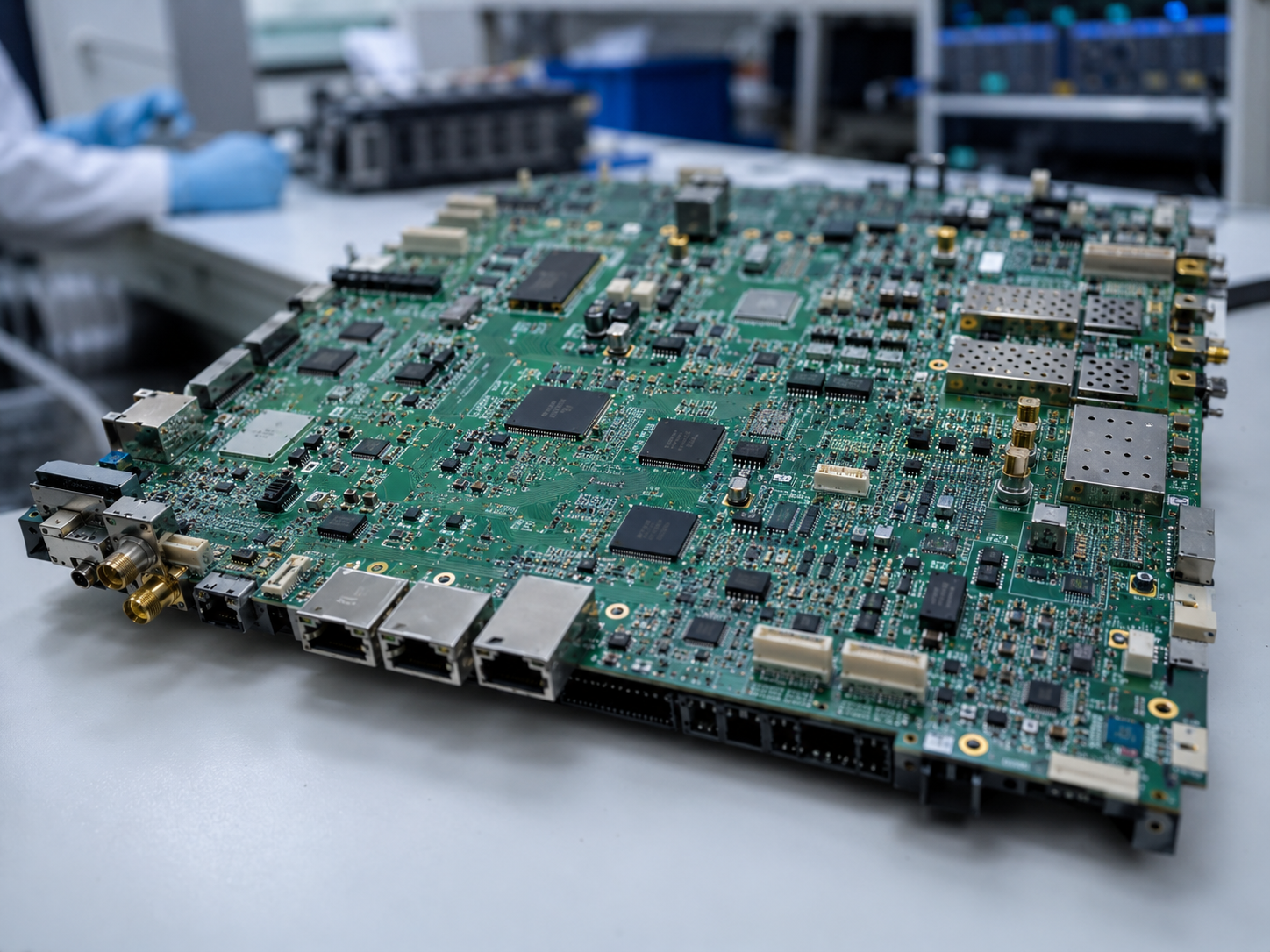
Telecom PCB manufacturing services encompass the full production process for printed circuit boards used in communication equipment. This typically includes PCB design review, material selection, prototyping, mass production, component sourcing, PCB assembly, inspection, testing, packaging, and delivery.
These services are not just about producing boards. They ensure that each PCB meets the required performance, reliability, and delivery standards. A competent supplier verifies board structure, material choice, copper thickness, surface finish, and manufacturing tolerances before production begins to prevent potential issues later.
A trusted telecom circuit board manufacturing partner also accommodates different project stages. Whether a project requires fast prototypes for validation or stable batch production for long-term supply, EBest supports the entire workflow, helping projects move smoothly from initial testing to full-scale production with minimal risk and clear communication.
Where Are Telecom PCBs Used in High-Speed Communication Equipment?
Telecom PCBs are used in communication devices that handle signal transmission, data processing, power control, and network connection. They help equipment maintain stable performance in high-speed and long-term operation.
5G Base Stations
Used in RF units, control boards, and signal processing modules to support stable wireless transmission.
Routers and Network Switches
Used for data routing, network control, and high-speed signal transmission.
Optical Communication Equipment
Used in optical modules, fiber optic devices, and transmission systems to support low-loss communication.
Wireless Communication Devices
Used in gateways, repeaters, terminals, and wireless modules for signal receiving and transmitting.
Network Servers and Data Systems
Used in servers, storage equipment, and data communication systems that require stable high-speed performance.
Antenna and RF Modules
Used in RF systems where impedance control, material stability, and low signal loss are important.
Industrial Communication Equipment
Used in industrial gateways, controllers, and remote monitoring devices for reliable network communication.

Why Do Telecom PCBs Require High Reliability and Signal Stability?
Telecom PCBs are essential for high-speed communication systems where even small signal interruptions can affect overall performance. Boards must maintain consistent electrical characteristics to ensure fast, accurate data transmission.
Precise impedance control, consistent layer alignment, and uniform material properties are critical. Variations in copper thickness, surface finish, or board structure can lead to signal degradation, crosstalk, or electromagnetic interference, impacting device performance.
These PCBs often operate continuously under demanding conditions including high temperatures and electrical load. Reliability ensures the board performs consistently over time without failure.
High reliability and signal stability allow communication equipment such as base stations, routers, optical modules, and RF devices to function efficiently, deliver accurate data, and maintain network integrity across all operating conditions.
What Technical Requirements Should Be Confirmed Before Telecom PCB Production?
Before starting production, key technical requirements should be clearly defined to ensure signal performance, reliability, and accurate assembly for telecom PCBs. For telecom pcb manufacturing services, these details help confirm whether the board can meet high-speed communication requirements before production begins.
| Technical Requirement | Typical Values |
|---|---|
| PCB Layer Count | 2, 4, 6, 8, 10, 12 layers |
| Base Material | FR4 Tg 130°C, FR4 Tg 170°C, Rogers 4350B, PTFE |
| Board Thickness | 0.4 mm, 0.6 mm, 0.8 mm, 1.0 mm, 1.6 mm |
| Copper Thickness | 1 oz/ft² 35 μm, 2 oz/ft² 70 μm, 3 oz/ft² 105 μm |
| Impedance Control | 50 Ω ±5%, 75 Ω ±5%, 100 Ω differential ±10% |
| Line Width / Spacing | Minimum 3 mil / 3 mil, 4 mil / 4 mil, 5 mil / 5 mil |
| Hole Size / Via | 0.2 mm to 1.0 mm, through-hole, blind via, buried via, microvia |
| Surface Finish | HASL, ENIG, OSP, immersion silver, immersion tin |
| Solder Mask | 15 to 20 μm thickness, green, blue, or black |
| Silkscreen | 0.1 mm line width, white or black ink |
| Assembly Method | SMT, through-hole, mixed technology |
| Testing Requirements | Flying probe, ICT, AOI, impedance test, functional test |
| Production Quantity | Prototype: 1 to 10 pcs, small batch: 10 to 500 pcs, mass production: over 500 pcs |
| Delivery Lead Time | Prototype: 1 to 3 weeks, small batch: 2 to 4 weeks, mass production: 4 to 8 weeks |
What Standards Should Telecom PCB Manufacturing Services Follow?
Telecom PCB manufacturing requires adherence to recognized quality, safety, and environmental standards to ensure reliable performance and long-term stability.
ISO 9001:2015
Focuses on overall quality management, ensuring consistent production processes and documentation control.
IPC Standards
Standards such as IPC-A-600, IPC-6012, and IPC-A-610 define PCB acceptability, performance requirements, and assembly quality, ensuring consistent manufacturing results.
UL Certification
Verifies product safety and material reliability, supporting compliance with international safety regulations.
RoHS Compliance
Limits the use of hazardous substances in PCBs, ensuring environmentally safe production for global markets.
REACH Compliance
Controls the use of chemical substances, promoting environmentally responsible PCB manufacturing.
IATF 16949
A standard primarily used for automotive-related PCBs. It ensures rigorous process control, traceability, and defect prevention.
ISO 13485
Applies to medical device-related PCBs. It emphasizes consistent production quality, risk management, and regulatory compliance.
AS9100D
Used in aerospace and defense PCB production. It focuses on process reliability, risk management, and quality control for high-performance applications.
What Challenges Are Common in Telecom PCB Manufacturing?
Telecom PCB manufacturing is more demanding than standard PCB production because communication equipment must handle fast signals, long operating hours, and stable data transmission. Even small process variations can affect signal quality, assembly reliability, or final product performance.
Signal Loss
High-speed signals can weaken during transmission if the material, stack-up, or trace design is not properly controlled. Low-loss materials and stable production processes help reduce this risk.
Impedance Control
Telecom PCBs often require controlled impedance, such as 50 Ω single-ended or 100 Ω differential impedance. If impedance values are not stable, signal reflection and transmission errors may occur.
Multilayer Alignment
Many telecom PCBs use multilayer structures to support complex routing and compact product design. Accurate layer alignment is important for stable connections, reliable vias, and consistent electrical performance.
High-Density Routing
Communication boards often include fine traces, small spacing, and dense component areas. This requires precise manufacturing capability to avoid short circuits, open circuits, and yield loss.
Thermal Management
Telecom equipment may work continuously under high load. Good heat control helps prevent material deformation, component stress, and long-term reliability issues.
Assembly Reliability
Fine-pitch components, BGAs, connectors, and RF modules require accurate placement and stable soldering. Poor assembly control can lead to weak solder joints, hidden defects, or unstable operation.
Testing Consistency
Telecom PCBs often require electrical testing, impedance testing, AOI, X-ray inspection, or functional testing. Consistent testing helps confirm board quality before shipment and reduces project risk.
How Does the Telecom PCB Manufacturing Process Work?
Telecom PCB production requires a controlled process because these boards are often used in high-speed, high-frequency, and long-term operating communication equipment. Each step must support stable signal transmission, accurate layer structure, reliable assembly, and consistent product quality.
Step 1: Production File Review
Production starts with checking Gerber files, drill files, stack-up, impedance requirements, material specifications, copper thickness, and surface finish. This step confirms whether the design is suitable for telecom PCB manufacturing before materials are prepared.
Step 2: Material Preparation
The required laminate, copper foil, prepreg, and core materials are prepared according to the project specifications. For telecom PCBs, material stability is important because it affects signal loss, impedance control, heat resistance, and long-term reliability.
Step 3: Inner Layer Imaging and Etching
For multilayer telecom PCBs, the inner circuit layers are first transferred onto copper-clad laminates. After imaging and etching, the inner layer circuits are inspected to ensure correct trace width, spacing, and pattern accuracy.
Step 4: Layer Lamination
The inner layers, prepreg, and copper foil are stacked and pressed together under controlled temperature and pressure. Accurate lamination helps maintain board thickness, layer alignment, and electrical stability.
Step 5: Drilling and Via Formation
Mechanical drilling or laser drilling is used to create through holes, blind vias, buried vias, or microvias. These vias build electrical connections between different layers and are especially important for dense telecom PCB designs.
Step 6: Copper Plating
After drilling, copper is deposited inside the holes and on the board surface. Good plating quality ensures reliable layer-to-layer connection, stable current flow, and long-term board durability.
Step 7: Outer Layer Circuit Formation
The outer layer circuit pattern is created through imaging, plating, and etching. For telecom PCBs, line width, spacing, and copper uniformity must be carefully controlled to support signal stability and production consistency.
Step 8: Solder Mask Application
Solder mask is applied to protect copper traces, prevent oxidation, and reduce the risk of solder bridging during assembly. Accurate solder mask openings are important for fine-pitch components and high-density communication boards.
Step 9: Surface Finish Treatment
Surface finishes such as ENIG, HASL, OSP, immersion silver, or immersion tin are applied to protect exposed copper and improve solderability. The right finish depends on assembly requirements, storage time, and product reliability needs.
Step 10: Electrical Test and Impedance Test
Telecom PCBs are tested for open circuits, short circuits, and electrical continuity. If controlled impedance is required, impedance testing is also performed to verify whether the board meets the target values.
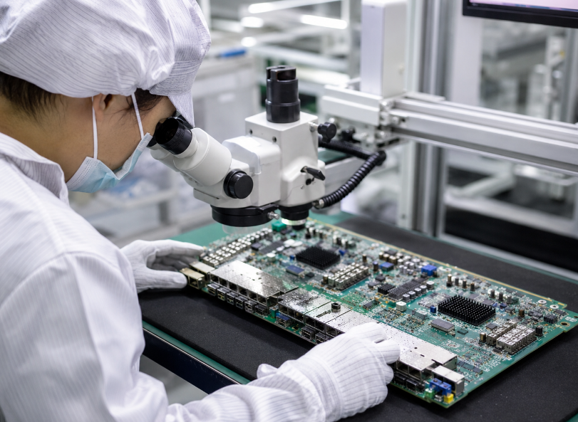
Step 11: PCB Assembly if Required
When the project includes assembly, the process continues with component sourcing, solder paste printing, SMT placement, reflow soldering, through-hole assembly, AOI inspection, X-ray inspection, and functional testing.
Step 12: Final Inspection and Packaging
Before delivery, the finished boards are checked for appearance, dimensions, markings, cleanliness, and packaging requirements. Proper packaging helps protect telecom PCBs from moisture, contamination, and handling damage during shipment.
What Telecom PCB Manufacturing Services Does EBest Offer?
EBest provides one-stop telecom pcb manufacturing services for communication equipment projects, covering PCB fabrication, assembly support, component sourcing, testing, and delivery coordination. These services help simplify project management from prototype to mass production.
PCB Design Support
EBest can support file review, DFM checking, stack-up discussion, and production feasibility confirmation before manufacturing begins.
PCB Prototype Production
Prototype service helps verify board structure, material selection, assembly fit, and basic performance before moving to larger production quantities.
Mass PCB Production
EBest supports stable batch production for telecom PCB orders that require consistent quality, repeatable processes, and long-term supply support.
Component Sourcing
For assembly projects, EBest can help source components according to the BOM, reducing coordination work and improving project efficiency.
PCB Assembly
EBest provides PCB assembly services, including SMT assembly, through-hole assembly, mixed assembly, inspection, and testing support.
High-Speed and RF PCB Manufacturing
EBest supports PCB projects that require high-speed materials, RF performance, impedance control, multilayer structures, and stable signal transmission.
HDI and Multilayer PCB Production
For compact communication equipment, EBest can support HDI and multilayer PCB production with fine routing, small vias, and dense circuit structures.
Testing and Inspection Support
Testing support can include electrical testing, AOI, X-ray inspection, impedance testing, functional testing, and other project-specific quality checks.
Expedited PCB Service
For urgent projects, EBest can support expedited production when files, materials, and production conditions are confirmed.
One-Stop Project Coordination
EBest helps coordinate PCB production, assembly, testing, packaging, and delivery through one supplier, reducing communication gaps and improving project control.
How Does EBest Control Quality in Telecom PCB Manufacturing?
EBest controls quality from the first review stage, not only at final inspection. For telecom pcb manufacturing services, our team checks Gerber files, stack up, impedance requirements, material selection, copper thickness, surface finish, and assembly details before production starts. This helps reduce hidden risks before the order enters manufacturing.
During production, EBest manages each key process carefully, including drilling, plating, lamination, imaging, solder mask, surface finish, routing, and assembly. For telecom PCBs, stable process control is essential because small variations may affect signal transmission, impedance consistency, and long term reliability.
Quality inspection is carried out through multiple steps according to project needs. Common checks include electrical testing, AOI inspection, impedance testing, visual inspection, dimensional inspection, X-ray inspection for assembled boards, and functional testing. These checks help confirm that each board meets the required specifications before shipment.
EBest also follows strict quality and compliance requirements for demanding PCB projects. With controlled production, inspection records, material traceability, and reliable testing support, EBest helps customers receive telecom PCBs with stable quality, lower rework risk, and stronger confidence for future repeat orders.
How Does EBest Ensure On-Time Delivery for Telecom PCB Orders?
EBest improves delivery reliability by confirming project details clearly before production starts. Gerber files, BOM, materials, copper thickness, surface finish, assembly needs, testing requirements, quantity, and target delivery date are reviewed in advance. Clear confirmation helps prevent delays caused by missing or unclear information.
Our integrated service also helps shorten the project cycle. EBest can coordinate PCB fabrication, component sourcing, PCB assembly, testing, packaging, and delivery in one workflow. This reduces communication gaps and keeps the project schedule easier to manage.
Production planning is arranged according to order urgency, material availability, process complexity, and testing requirements. Whether the project is a prototype, small batch, or repeat order, EBest works to keep each step moving smoothly while maintaining stable production quality.
For urgent telecom PCB projects, EBest can provide expedited service when files, materials, and production conditions are confirmed. Some urgent boards can be shipped within 24 hours, helping customers respond faster to sample approval, project deadlines, or unexpected production needs.
Why Choose EBest for Telecom PCB Manufacturing Services?
Choosing EBest for telecom pcb manufacturing services means working with a PCB manufacturing partner that helps reduce project risk, improve quality stability, and keep telecom PCB orders on schedule. For communication equipment projects, customers need reliable production, certified quality systems, strong process capability, and responsive project support.
Certified Quality Systems
EBest supports ISO 9001:2015, IATF 16949, ISO 13485:2016, AS9100D, UL, RoHS, and REACH. These certifications help customers reduce supplier evaluation risk and build confidence in long-term cooperation.
Strong Process Capability
Telecom PCBs may require multilayer structures, impedance control, high-speed signals, RF performance, HDI design, fine lines, and small vias. EBest supports these requirements for both standard and complex communication PCB projects.
One-Stop Service Support
EBest provides PCB design support, prototyping, mass production, component sourcing, PCB assembly, testing, packaging, and delivery coordination. This helps reduce communication errors and saves time compared with managing multiple suppliers.
Reliable Delivery Control
EBest supports standard production and expedited service for urgent orders. When files, materials, and production conditions are ready, urgent telecom PCB orders can move quickly to support tight project schedules.
Stable Quality from Sample to Batch Production
EBest focuses on material confirmation, process control, electrical testing, AOI inspection, impedance testing, X-ray inspection, and functional testing. This helps maintain consistent quality from prototypes to mass production.
Wide PCB Capability
EBest supports FR4 PCB, high Tg PCB, RF PCB, high-speed PCB, HDI PCB, multilayer PCB, metal core PCB, ceramic PCB, flexible PCB, rigid-flex PCB, heavy copper PCB, extra thin PCB, and impedance control PCB for different telecom applications.
Practical Cost Control
EBest helps customers choose suitable materials, processes, surface finishes, and testing methods based on actual project needs. This avoids unnecessary over-specification while keeping the required quality and reliability.
Responsive Communication
EBest provides clear feedback on manufacturability, material options, assembly needs, testing requirements, and delivery feasibility. This helps customers make faster decisions and move orders forward with greater confidence.
FAQs About Telecom PCB Manufacturing Services
Q1: What information is needed for a telecom PCB quotation?
A1: Please provide Gerber files, BOM, PCB specifications, material requirements, quantity, surface finish, testing needs, and expected delivery time. If assembly is required, placement files and component details should also be included.
Q2: Can telecom PCB production support both prototypes and mass production?
A2: Yes. A reliable telecom PCB supplier should support prototype validation, small batch production, and stable mass production. This helps projects move smoothly from sample testing to long-term supply.
Q3: What makes telecom PCBs different from standard PCBs?
A3: Telecom PCBs usually require better signal stability, impedance control, multilayer alignment, material stability, and testing accuracy. These requirements help support high-speed communication and long-term equipment operation.
Q4: What PCB types are commonly used in telecom equipment?
A4: Common options include multilayer PCB, high-speed PCB, RF PCB, HDI PCB, impedance control PCB, high Tg PCB, rigid-flex PCB, and metal core PCB. The right choice depends on signal speed, frequency, heat load, and product structure.
Q5: Does EBest provide PCB assembly for telecom projects?
A5: Yes. EBest supports PCB fabrication, component sourcing, SMT assembly, through-hole assembly, mixed assembly, inspection, testing, and delivery coordination. This helps simplify the full project process.
Q6: How does EBest help reduce telecom PCB project risk?
A6: EBest reviews files, materials, stack-up, impedance, assembly needs, and testing requirements before production. This helps identify risks early, reduce rework, and improve production stability.
Q7: Can EBest support urgent telecom PCB orders?
A7: Yes. EBest supports expedited production when files, materials, and production conditions are confirmed. This helps urgent prototypes or time-sensitive telecom PCB orders move forward faster.
How Can You Start Your Telecom PCB Project with EBest?
Starting your telecom PCB project with EBest is easy. Send your Gerber files, BOM, quantity, material requirements, surface finish, testing needs, assembly requirements, and target delivery time to sales@bestpcbs.com.
For reliable telecom pcb manufacturing services, EBest will review your project details, confirm production feasibility, and provide a clear quotation. Whether you need prototypes, batch production, PCB assembly, or urgent delivery, our team can help you move your telecom PCB project forward with reliable quality and professional support.
Tags: Telecom PCB Manufacturing, Telecom PCB Manufacturing Process, Telecom PCB Manufacturing Services, Telecom PCB Manufacturing Standard
PakarPBN
A Private Blog Network (PBN) is a collection of websites that are controlled by a single individual or organization and used primarily to build backlinks to a “money site” in order to influence its ranking in search engines such as Google. The core idea behind a PBN is based on the importance of backlinks in Google’s ranking algorithm. Since Google views backlinks as signals of authority and trust, some website owners attempt to artificially create these signals through a controlled network of sites.
In a typical PBN setup, the owner acquires expired or aged domains that already have existing authority, backlinks, and history. These domains are rebuilt with new content and hosted separately, often using different IP addresses, hosting providers, themes, and ownership details to make them appear unrelated. Within the content published on these sites, links are strategically placed that point to the main website the owner wants to rank higher. By doing this, the owner attempts to pass link equity (also known as “link juice”) from the PBN sites to the target website.
The purpose of a PBN is to give the impression that the target website is naturally earning links from multiple independent sources. If done effectively, this can temporarily improve keyword rankings, increase organic visibility, and drive more traffic from search results.
Comments are closed, but trackbacks and pingbacks are open.