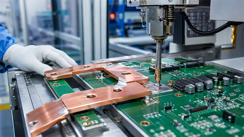
Copper bus bars are solid copper conductors used to carry and distribute high current with lower resistance, lower voltage drop, and better heat dissipation than many standard PCB copper traces. In PCB and PCBA applications, copper bus bars are often mounted onto exposed copper pads, soldered into power areas, mechanically fixed to the board, or integrated into a complete box build assembly.
In simple words, a copper bus bar works like a high-current electrical highway. Instead of forcing strong current through long, wide PCB traces, engineers use a copper bar to create a shorter, stronger, and more efficient current path.
At EBest Circuit (Best Technology), we support customers with PCB fabrication, component sourcing, PCBA assembly, copper bus bar integration, functional testing, and box build service. For high-current products, this one-stop capability helps customers reduce design risk, improve assembly reliability, and move from prototype to production more smoothly.
What Are Copper Bus Bars Used for in Electronics?
Copper bus bars are used in electronics to carry, collect, and distribute electrical current between power sources, PCB assemblies, batteries, connectors, terminals, power modules, and load devices. They are especially useful when the current is too high for ordinary PCB traces to handle efficiently.
In many electronic products, the power path is not a small signal route. It may connect an input power terminal to a power conversion circuit, a battery pack to a protection board, a charger circuit to an output connector, or a PCB assembly to a metal enclosure. In these situations, a copper bus bar can provide a low-resistance and mechanically stable current path.
Common applications include:
- High-current PCB power distribution
- Battery pack and BMS connection
- Charger PCB output connection
- Inverter and converter power paths
- Motor controller current transfer
- Industrial power module assembly
- Grounding and chassis bonding
- Energy storage system connection
- Power supply input and output connection
- Box build internal power connection
You may also see related terms such as busbar, busbars, electrical bus bars, bus bar copper, and bus bars copper. These terms are widely used in electrical systems. In PCB applications, the meaning is more specific. The copper bus bar must match the PCB pad design, soldering process, mechanical fixation, creepage and clearance requirements, thermal design, and final product structure.
A copper ground bus bar or copper grounding bus bar is mainly used to provide a stable grounding or bonding path. In electronic equipment, it can help reduce ground impedance, improve EMC performance, and create a reliable connection between the PCB, chassis, enclosure, or power ground.
For customers building high-current electronics, EBest Circuit (Best Technology) can review whether a copper bus bar is needed, whether a heavy copper PCB is enough, and how the bus bar should be assembled to the PCB for stable long-term performance.
What Is the Difference Between Copper Bus Bars and PCB Copper Traces?
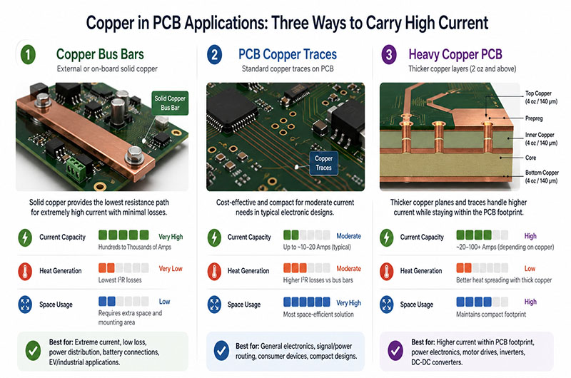
The main difference between copper bus bars and PCB copper traces is structure. PCB copper traces are flat conductive paths formed during PCB fabrication. Copper bus bars are separate solid copper conductors mounted onto or connected with the PCB assembly.
PCB traces are excellent for signals, control circuits, power planes, and moderate-current paths. Their current capacity depends on trace width, copper thickness, copper area, layer position, board material, airflow, and acceptable temperature rise.
Copper bus bars are used when the current path needs more cross-sectional copper area than a normal PCB trace can provide. Because the bus bar is thicker and stronger, it can carry more current while reducing voltage drop and heat concentration.
| Item | PCB Copper Traces | Copper Bus Bars |
|---|---|---|
| Structure | Flat copper pattern on PCB | Solid copper strip, bar, or formed conductor |
| Process | Made during PCB fabrication | Added during assembly or box build |
| Current capacity | Limited by trace width and copper weight | Higher due to larger copper cross-section |
| Thermal behavior | Depends on PCB copper area and stack-up | Better heat spreading in strong current paths |
| PCB space | May require very wide traces | Can save board routing space |
| Mechanical strength | Part of PCB laminate | Stronger, but needs reliable mounting |
| Best use | Signal, control, low to medium power | High-current power and grounding paths |
For example, a charger PCB may use normal copper traces for control signals, wider copper planes for power regulation, and a copper bus bar for the main output current path. This mixed structure makes the design more compact and practical.
From a manufacturing viewpoint, copper bus bars require more than a simple PCB layout. The PCB pad area, solder mask opening, surface finish, solder volume, heat control, fixture design, and inspection method must all be considered. This is why early DFM review is important before production.
EBest Circuit (Best Technology) provides DFM support before PCB fabrication and PCBA assembly. Our engineering team can help customers check whether the copper pad is large enough, whether the bus bar can be soldered properly, and whether additional mechanical fixation is needed.
Copper Bus Bars vs Heavy Copper PCB: What Is the Difference?
Copper bus bars and heavy copper PCBs both help carry higher current, but they solve the problem in different ways.
A heavy copper PCB increases the copper thickness inside or on the surface of the board. Instead of standard 1 oz or 2 oz copper, the board may use 3 oz, 4 oz, 6 oz, or higher copper weight. This allows PCB traces and copper planes to carry more current while staying integrated into the board.
A copper bus bar adds a separate copper conductor to the PCB or PCBA. It may be soldered onto exposed copper pads, fastened with screws, connected through terminals, or integrated into the final product structure.
Both options are useful. The best choice depends on current rating, board size, thermal design, production quantity, cost target, assembly structure, and reliability requirements.
| Comparison | Copper Bus Bars | Heavy Copper PCB |
|---|---|---|
| Current handling | Excellent for very high-current paths | Good for high-current PCB routing |
| PCB layout space | Can reduce wide trace requirements | May need large copper areas |
| Manufacturing complexity | Adds assembly process | Adds PCB fabrication complexity |
| Thermal performance | Strong heat spreading through solid copper | Good heat spreading through copper planes |
| Mechanical function | Can connect terminals, batteries, or modules | Mainly part of PCB circuit structure |
| Best for | Power terminals, battery paths, output bus, grounding | Integrated power planes and current routing |
Copper Bus Bars vs Heavy Copper PCB Cost Comparison
Cost should be evaluated from the whole product level, not only from the PCB price.
A heavy copper PCB may look simple because the copper is built into the board. But when copper thickness increases, PCB fabrication becomes more complex. Etching tolerance, solder mask coverage, lamination control, hole plating, and line spacing all become more demanding. For high layer count or very thick copper designs, PCB cost can rise quickly.
Copper bus bars add material and assembly cost, but they can reduce PCB size, avoid extreme copper thickness, and create a more direct current path. In some designs, using a copper bus bar with a moderate heavy copper PCB is more cost-effective than making the whole board with very thick copper.
A practical decision should consider:
- Required operating current
- Peak current and surge current
- Temperature rise limit
- PCB size and layout space
- Copper thickness requirement
- Bus bar material and plating
- Soldering or fastening method
- Assembly fixture cost
- Testing requirement
- Production quantity
- Long-term reliability target
EBest Circuit (Best Technology) has experience in both heavy copper PCB manufacturing and PCBA assembly. For high-current projects, we do not recommend one solution blindly. We review the current path, thermal condition, mechanical structure, and production process together, then suggest whether the design should use heavy copper PCB, copper bus bars, or a combined solution.
This engineering-first approach helps customers avoid overdesign, reduce unnecessary cost, and improve production reliability.
How Do Copper Bus Bars Affect PCB Layout?
Copper bus bars have a direct impact on PCB layout. They affect current flow, pad design, soldering area, mechanical clearance, thermal behavior, and inspection access.
The first layout concern is the current path. A copper bus bar should create a short and direct route between high-current nodes. If the bus bar is placed too far from the power path, or if the PCB copper connection under it is too narrow, current crowding may still occur.
The second concern is the pad structure. A soldered bus bar needs large exposed copper pads. The solder mask opening must be designed properly. The pad must provide enough area for solder wetting, current transfer, and mechanical bonding.
The third concern is thermal balance. Copper bus bars have high thermal mass. During soldering, they absorb heat quickly. If the heating process is not controlled well, the solder joint may be insufficient, or the PCB may suffer from thermal stress. The layout should support manufacturable soldering, not only electrical performance.
Important layout points include:
- Keep the high-current path short and direct.
- Use large copper pads under the bus bar.
- Avoid narrow copper neck-down areas.
- Provide proper solder mask opening.
- Consider thermal relief carefully.
- Maintain enough creepage and clearance.
- Leave mechanical space around the bus bar.
- Avoid placing heat-sensitive components nearby.
- Add mounting holes if screws or brackets are required.
- Ensure the solder joint can be inspected after assembly.
For box build products, the layout also needs to consider the enclosure, cable direction, heat sink, screws, insulation sheet, terminal block, and service access. A copper bus bar may fit perfectly on the PCB but still interfere with the housing or wiring if the whole product structure is not reviewed.
This is where EBest Circuit’s one-stop PCB, PCBA, and box build service can reduce communication loss. We can review the PCB layout, assembly process, and mechanical integration together, instead of treating them as separate steps.
What Is the Standard Soldering Method for PCB Copper Bus Bars?
The standard method for PCB copper bus bar assembly is usually soldering the copper bus bar onto large exposed PCB copper pads. The exact process depends on bus bar size, copper thickness, surface finish, solder alloy, PCB structure, and production volume.
Because copper has high thermal conductivity, bus bar soldering needs careful heat control. If the heating energy is too low, the solder may not wet properly. If the heating is too aggressive, the PCB laminate, solder mask, or nearby components may be affected.
Common soldering and attachment methods include:
- Selective soldering
- Manual soldering with controlled temperature tools
- Fixture-assisted soldering
- Hot bar soldering for suitable structures
- Reflow soldering for smaller or specially designed bus bars
- Wave soldering for certain through-hole bus bar designs
- Soldering combined with screws or mechanical fixation
How Are Copper Bus Bars Attached to PCB Pads?
Copper bus bars are commonly attached to PCB pads by soldering. The PCB is designed with large exposed copper pads, and the bus bar is placed onto these areas. Then solder is applied and heated to create a strong electrical and mechanical joint.
For larger bus bars, soldering alone may not be enough to handle mechanical stress. In these cases, screws, rivets, threaded inserts, standoffs, or brackets may be added. The solder joint provides electrical conductivity, while the mechanical structure helps absorb vibration, pulling force, or assembly stress.
This is especially important in automotive electronics, industrial control, power modules, and products with cable connections. If a cable pulls on the bus bar, the force should not be transferred only to the solder joint.
Are Copper Bus Bars Soldered or Welded to PCBs?
In most PCB and PCBA applications, copper bus bars are soldered to PCB pads rather than welded directly to the PCB.
Welding is more common for metal-to-metal joints, such as bus bar to battery tab, bus bar to copper terminal, bus bar to nickel strip, or bus bar to another metal conductor. Laser welding or resistance welding may be used in battery and power module manufacturing.
However, direct welding to a PCB is usually not recommended. PCB materials such as FR4, solder mask, copper foil, and plated layers are not designed for arc welding heat. Excessive heat can damage the laminate, reduce copper adhesion, burn the solder mask, deform the board, or affect nearby components.
Arc welding is generally not suitable for attaching copper bus bars directly to PCB pads. For PCB bus bar assembly, controlled soldering and mechanical fastening are usually safer and more manufacturable.
At EBest Circuit (Best Technology), we review the customer’s bus bar drawing, PCB files, pad design, plating requirement, and current rating before recommending the assembly method. Our goal is to help customers choose a process that is not only possible for one prototype, but also stable for repeat production.
What Industries Use PCB Copper Bus Bars?
PCB copper bus bars are used in industries where current density, heat control, voltage drop, and long-term reliability are important.
Electric vehicles and automotive electronics
Automotive products often need stable high-current paths in compact spaces. Copper bus bars may be used in onboard chargers, DC-DC converters, motor controllers, battery management systems, lighting modules, and power distribution units. These products also require vibration resistance, thermal stability, and traceable production.
Energy storage systems
Battery energy storage products use copper bus bars to connect battery modules, protection boards, current sensors, and power terminals. The design must consider current capacity, temperature rise, insulation, fastening, and service life.
Battery chargers and power supplies
Chargers, industrial power supplies, fast-charging equipment, and high-power adapters may use copper bus bars to reduce voltage drop and improve output current performance. In these products, soldering quality and thermal management are critical.
Industrial control
Motor drives, automation controllers, power control boards, and industrial switching modules may use copper bus bars to carry high current inside robust assemblies. Industrial customers often care about stable production quality, long product lifecycle, and reliable sourcing.
Telecommunications
Telecom power systems and base station power modules may use bus bars for low-resistance power distribution and grounding. Grounding busbars can also support EMC and system stability.
Medical electronics
Some medical power equipment and control modules require reliable current delivery, clean assembly, documentation, and traceability. For medical-related PCBA projects, manufacturing discipline is especially important.
Aerospace and high-reliability electronics
In demanding applications, copper bus bars may be used when current handling, weight, thermal performance, and mechanical reliability must be balanced carefully.
EBest Circuit (Best Technology) serves customers across industrial, medical, automotive, communication, and power electronics fields. With ISO 9001, ISO 13485, IATF 16949, AS9100D, UL, RoHS, and REACH-related quality experience, we understand that high-current PCB assembly is not only about conductivity. It is also about process control, documentation, traceability, and repeatable quality.
How Are Copper Bus Bars Integrated in PCBA and Box Build Projects?
Copper bus bars are often integrated during PCBA or box build assembly. In a complete product, the bus bar may connect the PCB to terminals, cables, batteries, power modules, heat sinks, grounding points, or metal enclosures.
A typical integration process includes:
Design and DFM review
The manufacturer reviews PCB files, bus bar drawings, copper thickness, current rating, pad design, surface finish, mounting structure, and soldering feasibility. Problems should be found before production, not after assembly.
PCB fabrication
The PCB is produced with the required copper thickness, pad openings, surface finish, mounting holes, and insulation design. For high-current boards, copper balance and warpage control also need attention.
Component sourcing and PCBA
Components are sourced and assembled through SMT, through-hole, selective soldering, or mixed assembly processes. For power electronics, component authenticity and BOM stability are also important.
Copper bus bar placement
The bus bar is placed onto the designed pad or mounting structure. Fixtures may be used to control alignment and repeatability.
Soldering or mechanical fastening
Depending on the product design, the bus bar may be soldered, screwed, riveted, or combined with multiple fixing methods.
Inspection and testing
The assembly is checked for solder wetting, alignment, contact condition, resistance, insulation, and function.
Box build assembly
The PCBA is installed into the enclosure. The bus bar may connect to external terminals, cable harnesses, grounding points, heat sinks, or power modules.
Final functional test
The finished product is tested before shipment to confirm that the complete assembly works as required.
EBest Circuit’s advantage is the ability to handle this process as a connected workflow. We are not only a PCB supplier. We support PCB fabrication, PCBA assembly, component procurement, testing, and box build integration. For customers developing high-current electronics, this reduces supplier coordination time and improves engineering communication.
What DFM Checks Are Needed Before Copper Bus Bar Assembly?
DFM review is essential before copper bus bar assembly. Small design issues can cause soldering defects, poor wetting, overheating, unstable resistance, or mechanical failure.
Before production, both the PCB and the bus bar structure should be reviewed.
| DFM Check Item | Why It Matters |
|---|---|
| Bus bar dimensions | Confirms fit, solder area, and clearance |
| Copper thickness | Affects current capacity and thermal behavior |
| PCB pad size | Determines solder joint strength and contact resistance |
| Surface finish | Affects solderability and oxidation resistance |
| Solder mask opening | Supports proper solder wetting |
| Mounting hole position | Ensures mechanical alignment |
| Creepage and clearance | Important for high-voltage safety |
| Component spacing | Avoids interference during assembly |
| Heat-sensitive parts | Reduces soldering damage risk |
| Solder volume | Supports reliable bonding |
| Fixture requirement | Improves production repeatability |
| Inspection access | Makes quality control easier |
Why tin plating on copper bus bars?
Tin plating is commonly used because it improves solderability and protects copper from oxidation. A tin plated copper bus bar is often easier to solder onto PCB pads than bare copper. For PCBA production, stable solder wetting is a major advantage.
Why silver plated copper bus bar?
Silver plating provides excellent conductivity and contact performance. A silver plated copper bus bar may be used in demanding electrical applications, but it is usually more expensive than tin plating. The decision should consider performance needs, environment, and budget.
What are copper bus bars made out of?
Copper bus bars are usually made from high-conductivity copper. The exact material grade, thickness, shape, and plating depend on current rating, thermal requirement, mechanical structure, and soldering process.
At EBest Circuit (Best Technology), our DFM support helps customers review these details before mass production. We can advise on PCB pad design, solder mask opening, surface finish, copper thickness, assembly method, and test strategy. This is especially helpful when customers are still moving from prototype design to stable production.
What Testing Is Needed for High-Current PCB Bus Bar Assembly?
High-current PCB bus bar assembly should be tested for electrical performance, thermal behavior, mechanical reliability, and assembly quality.
A board may pass a simple power-on test but still have hidden risks. For example, a weak bus bar solder joint may heat up under load. A narrow copper transition area may create local temperature rise. A mechanically unsupported bus bar may fail after vibration or repeated cable movement.
Common tests include:
Visual inspection
Checks solder wetting, alignment, pad coverage, solder cracks, contamination, and mechanical position.
Continuity test
Confirms that the bus bar is connected to the correct electrical net.
Contact resistance test
Measures the resistance of the bus bar connection. This is important because small resistance can create significant heat at high current.
High-current load test
Verifies whether the assembly can carry the required current under controlled conditions.
Temperature rise test
Measures heat buildup during operation. This test helps confirm whether the bus bar, solder joint, PCB copper, and surrounding components can work safely under real load.
Insulation resistance test
Checks isolation between high-current conductors and other circuits.
Hi-pot test
Used for high-voltage applications to verify insulation strength.
Vibration or mechanical stress test
Important for automotive, industrial, transportation, and outdoor products.
Thermal cycling test
Checks reliability under repeated temperature changes. This matters because copper, solder, and PCB laminate expand at different rates.
Functional test
Confirms that the full PCBA or box build performs as required.
EBest Circuit (Best Technology) supports multiple inspection and testing methods, including AOI, X-ray inspection where applicable, flying probe test, ICT, functional testing, burn-in support, and customized test fixtures. For high-current PCBA, we can work with customers to define the right test plan based on current level, application environment, and reliability target.
How to Choose the Right PCB Manufacturer for Copper Bus Bar Projects?
Choosing the right PCB manufacturer for copper bus bar projects requires more than checking whether the supplier can make a PCB. The manufacturer should understand high-current design, PCB fabrication limits, PCBA soldering process, mechanical integration, and final reliability testing.
A suitable supplier should be able to support:
- PCB fabrication with suitable copper thickness
- Heavy copper PCB when required
- Large exposed pad design review
- Copper bus bar soldering process evaluation
- Surface finish recommendation
- Component sourcing and BOM review
- High-current PCBA assembly
- Mechanical fastening review
- Thermal management suggestions
- Inspection and functional testing
- Box build assembly
- Production traceability
- Engineering communication before and during production
If your project includes a copper bus bar connector, battery bus bar copper part, copper grounding bus bar, tin plated copper bus bar, silver plated copper bus bar, or custom plated copper bus bar, the manufacturer should ask the right technical questions before quoting.
Useful project information includes:
- PCB Gerber files
- PCB stack-up
- Bus bar drawing
- Copper thickness
- Plating requirement
- Current rating
- Voltage rating
- Temperature rise limit
- Surface finish
- Soldering requirement
- Mechanical fastening design
- Enclosure or box build drawing
- Testing standard
- Production quantity
EBest Circuit (Best Technology) has more than 20 years of PCB and PCBA manufacturing experience. We support prototype, small-batch, and production projects for customers in industrial, medical, automotive, communication, power electronics, and other fields. Our service covers PCB fabrication, component sourcing, PCBA assembly, testing, and box build integration.
For high-current copper bus bar projects, this integrated capability helps customers reduce risk at the design stage, improve process stability during production, and simplify supplier management.
In summary, copper bus bars are widely used in high-current PCB and PCBA applications because they provide a stronger current path, lower resistance, lower voltage drop, and better thermal performance than many ordinary PCB traces. They are commonly used in chargers, inverters, battery systems, power supplies, motor controllers, industrial electronics, and energy storage products.
For PCB applications, copper bus bars are usually soldered onto large exposed copper pads or combined with mechanical fastening. Heavy copper PCB can replace copper bus bars in some designs, but many high-current products benefit from using both together. Arc welding is generally not suitable for direct PCB attachment because it may damage the board structure.
For customers, the success of a copper bus bar project depends on more than the copper part itself. It depends on PCB design, pad structure, copper thickness, surface finish, soldering process, inspection, testing, and final product integration.
EBest Circuit (Best Technology) provides one-stop support for PCB fabrication, PCBA assembly, component sourcing, copper bus bar integration, testing, and box build assembly. With strong engineering support, strict process control, and experience in high-current electronics, we help customers turn copper bus bar PCB designs into reliable finished products.
If you are developing a PCB or PCBA project with copper bus bars, heavy copper circuits, high-current power paths, or box build integration, pls feel free to contact EBest Circuit (Best Technology) via sales@bestpcbs.com for engineering review and quotation.
FAQs About Copper Bus Bars on PCBs
Can heavy copper PCB replace copper bus bars?
Yes, heavy copper PCB can replace copper bus bars in some designs, especially when current is moderate and the PCB has enough space for wide copper areas. For very high-current paths, compact layouts, power terminals, or battery connections, copper bus bars may still be a better choice. Many reliable products use both heavy copper PCB and copper bus bars together.
Are copper bus bars usually soldered onto PCB pads?
Yes. In many PCB and PCBA applications, copper bus bars are soldered onto large exposed PCB copper pads. For larger or mechanically stressed structures, soldering may be combined with screws, rivets, or brackets.
Can copper bus bars be arc-welded to a PCB?
Arc welding is generally not recommended for direct PCB attachment. The heat can damage FR4 laminate, solder mask, copper adhesion, plated holes, and nearby components. For PCB bus bar assembly, controlled soldering and mechanical fastening are usually more suitable.
Tags: Copper Bus Bars, electrical bus bars, pcb copper bus bar manufacturers
PakarPBN
A Private Blog Network (PBN) is a collection of websites that are controlled by a single individual or organization and used primarily to build backlinks to a “money site” in order to influence its ranking in search engines such as Google. The core idea behind a PBN is based on the importance of backlinks in Google’s ranking algorithm. Since Google views backlinks as signals of authority and trust, some website owners attempt to artificially create these signals through a controlled network of sites.
In a typical PBN setup, the owner acquires expired or aged domains that already have existing authority, backlinks, and history. These domains are rebuilt with new content and hosted separately, often using different IP addresses, hosting providers, themes, and ownership details to make them appear unrelated. Within the content published on these sites, links are strategically placed that point to the main website the owner wants to rank higher. By doing this, the owner attempts to pass link equity (also known as “link juice”) from the PBN sites to the target website.
The purpose of a PBN is to give the impression that the target website is naturally earning links from multiple independent sources. If done effectively, this can temporarily improve keyword rankings, increase organic visibility, and drive more traffic from search results.
Comments are closed, but trackbacks and pingbacks are open.