Ceramic PCB board is a high-performance circuit board built on a ceramic substrate instead of a conventional glass-fiber epoxy base. It is often selected when an electronic product needs excellent heat dissipation, dimensional stability, high insulation strength, and long-term reliability under demanding operating conditions. For aerospace electronics, power modules, RF devices, LED systems, medical equipment, and high-temperature industrial applications, ceramic circuit boards offer a strong foundation for designs where thermal and electrical performance matter from the first prototype to full production.
EBest Circuit (Best Technology) supports ceramic PCB fabrication, ceramic PCB prototype builds, ceramic substrate circuit board PCB PCBA projects, and engineering-driven manufacturing support for customers who need stable, production-ready solutions.
What Is a Ceramic PCB Board?
Ceramic PCB board is a printed circuit board that uses ceramic as the base substrate. The ceramic layer replaces the traditional FR4 laminate and provides stronger thermal conductivity, higher temperature resistance, and better electrical insulation. Conductive traces are formed on the ceramic surface through copper bonding, thick-film printing, thin-film metallization, or direct plated copper processes, depending on the application and performance target.
The main role of a ceramic PCB is to carry electronic circuits while also helping the product handle heat, stress, and electrical load more effectively. This makes it valuable for applications where a normal FR4 PCB may not provide enough thermal transfer or dimensional stability.
Ceramic circuit boards are often used in devices that must remain reliable for many years. These include aerospace power modules, RF amplifiers, laser systems, LED lighting modules, semiconductor test equipment, medical sensors, and industrial control products.
A ceramic PCB board may be supplied as a bare ceramic circuit board or as a fully assembled PCBA. A bare PCB board ceramic substrate includes the ceramic base, copper circuits, vias or pads if required, surface finish, and final inspection. A completed ceramic PCBA adds components, soldering, inspection, testing, and packaging. This full-process capability is useful when a customer wants one supplier to control fabrication, component sourcing, assembly, and quality verification.
How Is a Ceramic PCB Board Different from a Standard FR4 PCB?
Ceramic PCB board and an FR4 PCB both provide electrical interconnection, but they are designed for different performance levels. FR4 is a glass-reinforced epoxy laminate widely used in consumer electronics, control boards, communication devices, and general industrial products. It is affordable, easy to process, and suitable for many standard designs.
The biggest difference is the substrate. FR4 has relatively low thermal conductivity. It can work very well in many electronic products, but it does not move heat as quickly as ceramic. Ceramic materials such as aluminum nitride and alumina provide much stronger thermal paths.
| Comparison Item | Ceramic PCB Board | Standard FR4 PCB |
|---|---|---|
| Base Material | Alumina, aluminum nitride, silicon nitride, or other ceramic substrate | Glass fiber reinforced epoxy laminate |
| Thermal Conductivity | High to very high, depending on ceramic material | Low, usually suitable for moderate heat loads |
| Temperature Resistance | Excellent for high-temperature environments | Good for standard electronics, limited at higher temperatures |
| Electrical Insulation | Strong insulation with good dielectric strength | Good insulation for common circuit designs |
| Dimensional Stability | Very stable under heat | More expansion under thermal stress |
| Typical Applications | Aerospace, power electronics, RF, LED, medical, laser, semiconductor modules | Consumer electronics, general industrial boards, communication products |
| Cost Level | Higher because of material and process complexity | Lower and widely available |
| Prototype Consideration | Requires careful design review and manufacturer experience | Faster and easier for common PCB factories |
| Assembly Needs | Requires controlled soldering and thermal process knowledge | Mature and common SMT process flow |
The choice is not about which material is always better. It is about whether the design needs the extra performance. For a simple control board with low heat, FR4 is often a smart choice. For a compact power module or aerospace AlN ceramic PCB board, ceramic can offer a stronger long-term solution.
What Are Ceramic Circuit Boards Used For?
Ceramic circuit boards are used in products where heat, power density, precision, and reliability must be controlled carefully. They are often found in industries that value stable performance over the full product life cycle.
In aerospace electronics, ceramic boards are used in power control modules, RF communication devices, sensor systems, radar-related circuits, and high-reliability control units. These products often work in environments with temperature changes, vibration, and strict weight limitations. A ceramic PCB can help engineers reduce thermal stress and improve circuit stability.
In power electronics, ceramic circuit boards are used for MOSFETs, IGBTs, power converters, motor drives, solid-state relays, and high-current modules. The ceramic substrate helps transfer heat from the power device to the heat spreader or housing. This supports smaller designs and more stable operating temperatures.
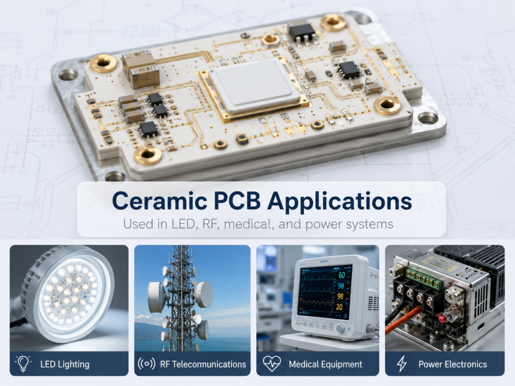
Common applications include:
- Aerospace power modules, RF units, avionics sensors, and satellite-related electronic assemblies.
- High-power LED modules, UV LED curing systems, automotive lighting, and industrial lighting engines.
- RF and microwave circuits, including amplifiers, filters, antennas, and high-frequency ceramic substrate modules.
- Medical electronics such as imaging equipment, sensor modules, laser systems, and diagnostic devices.
- Semiconductor equipment, probe cards, laser diode carriers, and precision measurement instruments.
- New energy products, charging modules, power conversion units, and thermal management assemblies.
Ceramic PCB boards are also widely used in high-end lighting. For example, LED chips generate concentrated heat. If that heat stays near the junction, brightness and life span can be affected. In RF applications, ceramic materials offer stable dielectric behavior. This is useful for circuits where signal loss, impedance control, and frequency stability are important.
What Ceramic PCB Materials Are Commonly Used?
The most common ceramic PCB materials include alumina, aluminum nitride, silicon nitride, and sometimes beryllium oxide in special legacy or niche applications. For modern commercial and industrial projects, alumina and aluminum nitride are the most widely used because they offer a practical balance of performance, manufacturability, availability, and cost.
Alumina ceramic, often written as Al₂O₃, is the most familiar option. It offers good insulation, good mechanical strength, stable performance, and a cost level that is more accessible than aluminum nitride. Common purities include 96% alumina and 99% alumina.
Aluminum nitride, written as AlN, is used when much higher thermal conductivity is required. Some buyers may search for an “aluminum nitride AIN ceramic PCB board,” although the correct chemical abbreviation is AlN. This material is especially attractive for aerospace, high-power LED, RF, laser, and power semiconductor applications. It offers excellent heat transfer while maintaining electrical insulation.
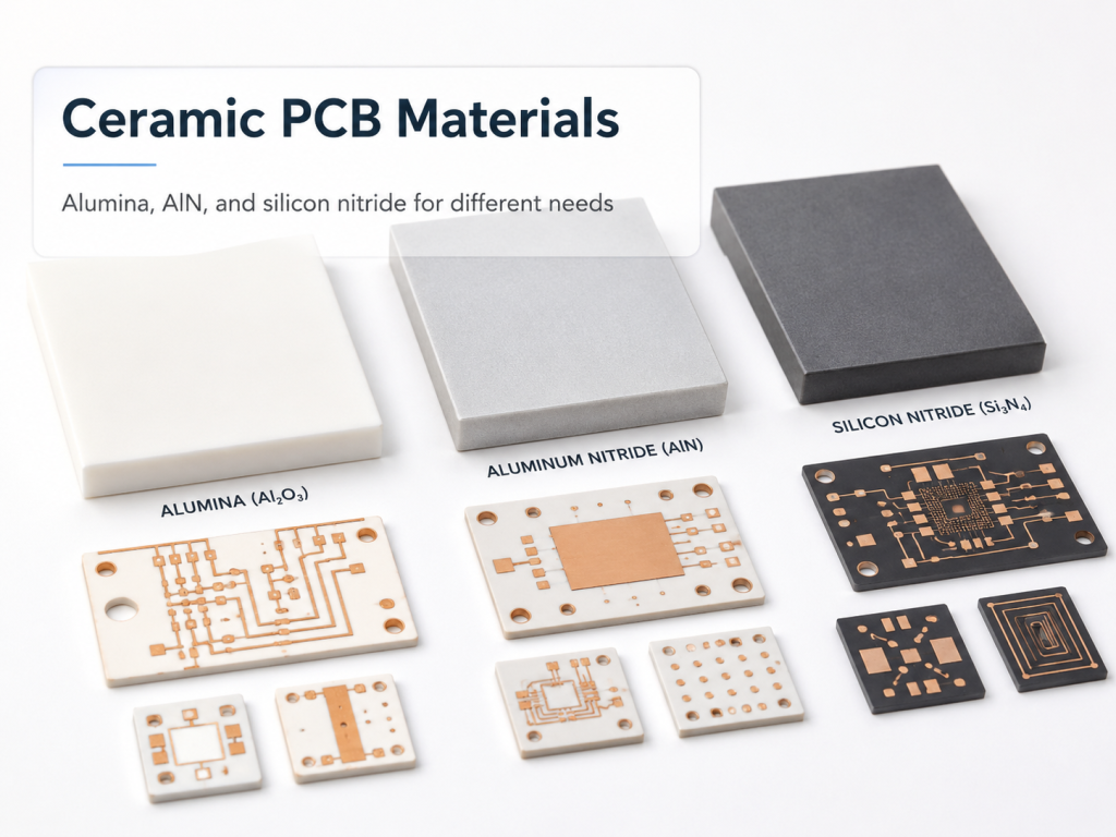
Silicon nitride is known for strong mechanical toughness and thermal shock resistance. It can be useful in applications where the board may face mechanical stress, impact risk, or repeated heating and cooling.
A simple way to view the material choices is this:
| Ceramic PCB Material | Main Strength | Typical Use Case | Cost Tendency |
|---|---|---|---|
| 96% Alumina | Good insulation, stable processing, balanced cost | LED modules, sensors, industrial electronics, general ceramic PCB prototype | Moderate |
| 99% Alumina | Better purity, stronger electrical performance | Precision circuits, medical modules, high-reliability electronics | Moderate to higher |
| Aluminum Nitride | Excellent thermal conductivity | Aerospace, power modules, RF, laser diodes, high-power LED | Higher |
| Silicon Nitride | High toughness and thermal shock resistance | Harsh mechanical or thermal environments | Higher |
| Beryllium Oxide | Very high thermal performance but special handling concerns | Limited specialized applications | Special-case material |
When selecting ceramic PCB materials, engineers should not only compare thermal conductivity values. They should also review copper bonding method, via structure, surface finish, operating voltage, component type, board size, tolerance, and assembly process.
What Is an Aluminum Nitride AlN Ceramic PCB Board?
An aluminum nitride AlN ceramic PCB board is a circuit board made with an AlN ceramic substrate. It is selected mainly for its excellent thermal conductivity and strong electrical insulation. For products that generate concentrated heat, AlN can help transfer heat away from components while still keeping the circuit electrically isolated.
AlN ceramic PCB boards are often used in aerospace electronics, laser diode modules, RF power amplifiers, high-brightness LED systems, power semiconductor packages, and new energy modules. In these products, heat is not just a side issue. It is one of the main factors that shapes the product’s service life, efficiency, and safety margin.
Aerospace applications are a strong fit for AlN because engineers often need compact and lightweight solutions. They also need materials that can perform through temperature changes and long operating cycles. An aerospace AlN ceramic PCB board can support this goal by combining thermal efficiency with a stable ceramic platform.
However, AlN projects require careful manufacturing control. The material is harder and more brittle than organic laminates, so drilling, cutting, metallization, and handling must be done with suitable process knowledge. Copper adhesion, surface flatness, laser processing, and final inspection are also important.
EBest Circuit supports aluminum nitride ceramic PCB manufacturing for customers who need high thermal performance, stable process control, and engineering communication during the design-to-production stage. For aerospace or other high-reliability projects, early DFM review is especially useful because it can help refine copper layout, board thickness, surface finish, and assembly method before production begins.
When Should You Choose Alumina Ceramic PCB Materials?
Alumina ceramic PCB materials are a strong choice when the design needs better thermal performance than FR4, good electrical insulation, stable mechanical properties, and a more economical ceramic option than AlN. Alumina is widely used because it offers a practical balance between performance and cost.
You may choose alumina when the heat load is moderate to high but does not require the premium thermal performance of aluminum nitride. It is common in LED modules, sensor boards, power control circuits, thick-film ceramic circuits, medical devices, and industrial electronics.
Alumina is available in different purity levels. A 96% alumina ceramic substrate is popular because it is cost-effective and reliable for many applications. A 99% alumina substrate can offer better purity and performance for more demanding circuits.
Before choosing alumina, engineers should review several points:
- Thermal requirement: Alumina is better than FR4, but AlN is stronger for very high heat transfer.
- Circuit density: Fine traces may require a more precise metallization process.
- Operating environment: Alumina performs well in high-temperature and stable insulation applications.
- Cost target: Alumina often supports a more controlled ceramic board price than premium ceramic materials.
- Assembly plan: Component size, soldering profile, and thermal mass should be reviewed early.
Alumina is also suitable for ceramic PCB prototype projects. When a customer wants to validate a ceramic design before mass production, alumina can provide a dependable starting point. It allows engineers to test thermal behavior, mechanical fit, surface finish, solderability, and electrical function without immediately moving to a more expensive material.
What Is a Bare PCB Board Ceramic Substrate?
A bare PCB board ceramic substrate is a ceramic circuit board before electronic components are assembled. It includes the ceramic base, conductive circuits, pads, vias if required, and surface finish.
For a ceramic PCB, the bare board stage is especially important. The substrate material, copper bonding, circuit pattern accuracy, hole quality, surface finish, and inspection process all affect the final PCBA. If the bare ceramic circuit board is not controlled properly, assembly yield and long-term reliability can be affected.
A bare ceramic board may use several circuit-forming technologies. Thick-film ceramic circuits are made by printing conductive paste and firing it at high temperature. Thin-film ceramic circuits use vacuum deposition and etching to create fine patterns. DBC, or direct bonded copper, bonds copper directly to ceramic at high temperature and is often used for power modules. DPC, or direct plated copper, can create more precise copper features and plated vias for advanced designs.
The surface finish is also important. Common options may include ENIG, silver, gold plating, nickel plating, or other finishes depending on soldering and bonding needs. For wire bonding, the finish must support reliable bond strength.
A bare PCB board ceramic product is often ordered by customers who handle assembly internally or send it to another EMS provider. However, many customers now prefer one-stop support because ceramic boards require closer coordination between fabrication and assembly.
EBest Circuit provides bare ceramic PCB board manufacturing as well as assembled ceramic PCBA service. This helps customers move from ceramic substrate design to finished electronic module with better process continuity.
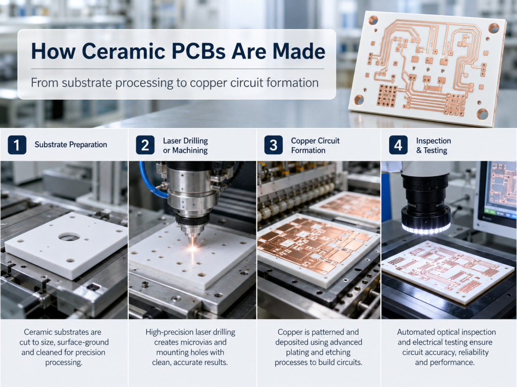
How Is a PCB Ceramic Circuit Board Manufactured?
A PCB ceramic circuit board is manufactured through a controlled process that depends on the ceramic material, copper structure, circuit density, and end application.
The manufacturing journey usually begins with engineering review. The manufacturer checks the Gerber files, stackup, substrate material, copper thickness, hole design, surface finish, tolerances, and assembly requirements. After the review, the ceramic substrate is prepared. The substrate must meet thickness, flatness, and surface quality requirements. Depending on the process, the circuit layer may be created by printing conductive paste, bonding copper foil, sputtering metal layers, or plating copper.
Typical manufacturing steps include:
- Material selection and DFM review based on thermal, electrical, and mechanical requirements.
- Ceramic substrate preparation, cleaning, thickness control, and surface inspection.
- Circuit formation through thick film, thin film, DBC, DPC, or another suitable process.
- Hole processing, laser drilling, mechanical drilling, or via formation where required.
- Copper patterning, etching, plating, or metallization control according to the design.
- Surface finish application for soldering, wire bonding, or corrosion protection.
- Electrical test, dimensional inspection, visual inspection, and packaging.
For DBC ceramic boards, copper is bonded to ceramic at high temperature. This method is excellent for power electronics because it supports thicker copper and strong thermal paths. For DPC ceramic boards, copper is built through plating, which can support finer features and plated vias. For thin-film ceramic boards, the process can create very precise patterns for RF, sensor, and high-frequency applications.
Can Ceramic PCB Boards Support PCBA Assembly?
Yes, ceramic PCB boards can support PCBA assembly, and many ceramic projects are built as complete assembled modules. In fact, ceramic substrates are often selected because they provide a better base for high-power components, LEDs, RF devices, sensors, and semiconductor packages.
Ceramic PCBA assembly requires more process attention than standard FR4 assembly. The board has different thermal behavior, higher rigidity, and lower flexibility. Soldering profiles must be controlled carefully because ceramic substrates conduct and absorb heat differently. Components with large thermal pads, power packages, or bottom terminations may need special stencil design and solder paste control.
SMT assembly on ceramic boards can include LEDs, ICs, resistors, capacitors, MOSFETs, sensors, connectors, and custom components. Some designs may also use wire bonding, die attachment, or hybrid assembly methods.
For ceramic substrate circuit board PCB PCBA projects, the best results usually come from close cooperation between the board manufacturer and assembly team. Pad design, surface finish, solder paste type, reflow curve, component thermal path, and inspection method should be considered together. A ceramic PCB can also support testing after assembly. Depending on the product, testing may include visual inspection, AOI, X-ray inspection, electrical testing, functional testing, thermal testing, or reliability screening..
EBest Circuit (Best Technology) offers one-stop PCB and PCBA manufacturing support, including ceramic PCB fabrication, component sourcing, SMT assembly, testing, and engineering communication. For customers who need both bare board ceramic substrates and assembled modules, this integrated support can reduce coordination gaps and help the project move faster from prototype to production.
How Do You Choose a Reliable Ceramics PCB Board Manufacturer?
Choosing a reliable ceramics PCB board manufacturer requires more than comparing unit price. Ceramic boards involve special materials, precision processing, thermal design, and assembly knowledge. A low quote may look attractive at the beginning, but the real value comes from stable quality, clear communication, process capability, and the ability to support your product through prototype and production.
First, review the manufacturer’s ceramic material experience. A capable supplier should understand alumina, aluminum nitride, and other ceramic PCB materials. They should be able to explain which material fits your application and why.
Second, check the process capability. Different ceramic circuit boards may require DBC, DPC, thick-film, thin-film, laser drilling, copper plating, precision cutting, or special surface finishes.
Third, evaluate engineering support. Ceramic PCB designs often benefit from DFM review before production. A good engineering team can help check pad design, thermal path, board thickness, surface finish, panelization, and manufacturability.
Fourth, confirm quality control and traceability. For aerospace, medical, industrial, and power electronics, documentation matters. Inspection records, material control, electrical testing, dimensional reports, and production traceability can give customers more confidence.
EBest Circuit (Best Technology) is positioned as an engineering-driven PCB and PCBA manufacturing partner. The company supports ceramic PCB board fabrication, ceramic circuit boards, ceramic PCB prototype builds, PCB ceramic circuit board production, component sourcing, PCBA assembly, and testing. For customers working on aerospace AlN ceramic PCB boards, LED thermal modules, power electronics, medical devices, or industrial control products, EBest provides practical support from design review to production delivery.
For ceramic PCB board manufacturing, ceramic PCB prototype support, or ceramic PCB PCBA assembly, you can contact EBest Circuit (Best Technology) at sales@bestpcbs.com
Tags: ceramic board price, ceramic circuit boards, ceramic pcb board, ceramic PCB materials, Ceramic PCB Prototype
PakarPBN
A Private Blog Network (PBN) is a collection of websites that are controlled by a single individual or organization and used primarily to build backlinks to a “money site” in order to influence its ranking in search engines such as Google. The core idea behind a PBN is based on the importance of backlinks in Google’s ranking algorithm. Since Google views backlinks as signals of authority and trust, some website owners attempt to artificially create these signals through a controlled network of sites.
In a typical PBN setup, the owner acquires expired or aged domains that already have existing authority, backlinks, and history. These domains are rebuilt with new content and hosted separately, often using different IP addresses, hosting providers, themes, and ownership details to make them appear unrelated. Within the content published on these sites, links are strategically placed that point to the main website the owner wants to rank higher. By doing this, the owner attempts to pass link equity (also known as “link juice”) from the PBN sites to the target website.
The purpose of a PBN is to give the impression that the target website is naturally earning links from multiple independent sources. If done effectively, this can temporarily improve keyword rankings, increase organic visibility, and drive more traffic from search results.
Comments are closed, but trackbacks and pingbacks are open.